Introduction to PDS Impedance
PDS (Power Distribution System) impedance is a critical factor in the design and optimization of power distribution networks in electronic systems. It refers to the combined resistance, inductance, and capacitance of the conductors, components, and interconnects that make up the power delivery path from the voltage regulator module (VRM) to the load devices, such as processors, FPGAs, or ASICs.
PDS impedance plays a vital role in determining the quality and stability of the power supply, as well as the overall performance and reliability of the system. High PDS impedance can lead to various issues, including:
- Voltage droops and overshoots during load transients
- Increased power supply noise and ripple
- Electromagnetic interference (EMI) and compatibility problems
- Reduced power efficiency and increased heat generation
Therefore, it is essential for hardware designers and engineers to carefully analyze and optimize PDS impedance throughout the design process. This article will explore the traditional approach to PDS design, its limitations, and how an energy flow-based approach can provide a more comprehensive and effective solution.
Traditional Approach to PDS Design
Lumped Element Model
The traditional approach to PDS design relies heavily on the lumped element model, which represents the power distribution network as a simplified circuit consisting of discrete components, such as resistors, inductors, and capacitors. This model is based on the assumption that the wavelengths of the signals propagating through the network are much larger than the physical dimensions of the components and interconnects.
In the lumped element model, the PDS is typically divided into several sections, each represented by a combination of R, L, and C elements. For example, the VRM output capacitance, the bulk decoupling capacitors, the printed circuit board (PCB) planes, and the package and die capacitance are all modeled as separate lumped elements.
Table 1: Lumped Element Representation of PDS Components
| Component | Lumped Element Representation |
|---|---|
| VRM Output Capacitance | Capacitor (C) |
| Bulk Decoupling Capacitors | Capacitor (C) |
| PCB Planes | Resistor (R) + Inductor (L) |
| Package and Die Capacitance | Capacitor (C) |
Frequency Domain Analysis
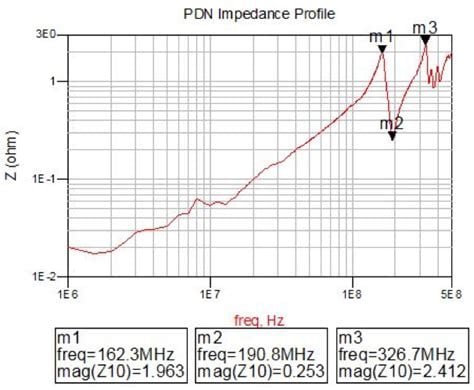
Using the lumped element model, PDS impedance is typically analyzed in the frequency domain using tools such as Spice or Ansys SIwave. The goal is to ensure that the impedance profile of the PDS remains below the target impedance curve across the frequency range of interest, which is determined by the current draw and transient response requirements of the load devices.
The target impedance curve is derived from the maximum allowable voltage ripple and the expected current transients, using the following equation:
Z_target = ΔV_max / ΔI_max
Where:
– Z_target is the target impedance
– ΔV_max is the maximum allowable voltage ripple
– ΔI_max is the maximum expected current transient
By comparing the simulated PDS impedance profile with the target impedance curve, designers can identify potential issues and optimize the PDS design by adjusting the values and placement of decoupling capacitors, modifying the PCB layout, or using alternative packaging technologies.
Limitations of the Traditional Approach
While the traditional approach to PDS design has been widely used in the industry, it has several limitations that can lead to suboptimal designs and increased risk of power integrity issues:
-
Inaccurate representation of distributed effects: The lumped element model assumes that the PDS components and interconnects are electrically small compared to the wavelengths of the signals. However, as signal frequencies continue to increase and rise times decrease, this assumption becomes less valid, and distributed effects, such as transmission line behavior and resonances, become more prominent. Ignoring these effects can result in significant discrepancies between the simulated and actual PDS impedance profiles.
-
Limited consideration of layout and geometry: The lumped element model does not fully capture the impact of the physical layout and geometry of the PDS components and interconnects on the impedance profile. Factors such as the shape and size of the PCB planes, the via geometry, and the placement of decoupling capacitors can significantly affect the PDS impedance, but are not accurately represented in the lumped element model.
-
Inadequate treatment of broadband noise: The traditional approach focuses primarily on the impedance profile at specific frequencies, such as the fundamental switching frequency of the VRM or the resonant frequencies of the decoupling capacitors. However, it does not adequately address the broadband noise that can occur due to the interaction between the PDS and the load devices, which can lead to signal integrity issues and EMI problems.
-
Lack of system-level optimization: The traditional approach often treats the PDS design as a separate task from the overall system design, leading to suboptimal trade-offs between power integrity, signal integrity, and other performance metrics. A more holistic approach that considers the interactions between the PDS and other system components, such as the package, the die, and the I/O interfaces, is necessary to achieve the best possible performance and reliability.
Energy Flow-Based Approach to PDS Design
To overcome the limitations of the traditional approach, an energy flow-based approach to PDS design has been gaining traction in recent years. This approach considers the PDS as a distributed network of energy storage and dissipation elements, and analyzes the flow of energy through the network in both the time and frequency domains.
Distributed Energy Storage and Dissipation Model
In the energy flow-based approach, the PDS is modeled as a distributed network of energy storage and dissipation elements, rather than a collection of lumped R, L, and C components. The energy storage elements include the magnetic fields in the inductors and the electric fields in the capacitors, while the energy dissipation elements include the resistive losses in the conductors and the dielectric losses in the insulators.
The distributed nature of the energy storage and dissipation elements is captured using a transmission line model, which takes into account the spatial variation of the electromagnetic fields along the length of the conductors and interconnects. This allows for a more accurate representation of the distributed effects, such as the propagation delay, the characteristic impedance, and the reflections at the boundaries.
Table 2: Distributed Energy Storage and Dissipation Elements in PDS
| Element | Energy Storage | Energy Dissipation |
|---|---|---|
| Conductors | Magnetic field (inductance) | Resistive losses |
| Dielectrics | Electric field (capacitance) | Dielectric losses |
| Decoupling Capacitors | Electric field (capacitance) | ESR and ESL |
| VRM Output Capacitance | Electric field (capacitance) | ESR and ESL |
Time-Frequency Analysis
In addition to the frequency domain analysis used in the traditional approach, the energy flow-based approach also employs time domain analysis to capture the transient behavior of the PDS. This is particularly important for understanding the interactions between the PDS and the load devices, which often involve fast current transients and complex power state transitions.
The time-frequency analysis is typically performed using techniques such as the wavelet transform or the short-time Fourier transform (STFT), which provide a multi-resolution representation of the signals in both the time and frequency domains. This allows for the identification of localized events, such as voltage droops or overshoots, as well as the characterization of the broadband noise spectrum.
System-Level Optimization
One of the key advantages of the energy flow-based approach is its ability to enable system-level optimization of the PDS design. By considering the interactions between the PDS and other system components, such as the package, the die, and the I/O interfaces, designers can make informed trade-offs between power integrity, signal integrity, and other performance metrics.
This holistic approach involves the co-design and co-simulation of the PDS with the rest of the system, using tools such as Ansys PowerArtist or Cadence Sigrity. These tools allow designers to explore various design options and optimize the PDS impedance profile, the decoupling capacitor placement, and the PCB layout in the context of the overall system performance.
Benefits of the Energy Flow-Based Approach
The energy flow-based approach to PDS design offers several benefits over the traditional approach:
-
Accurate representation of distributed effects: By using a transmission line model and considering the spatial variation of the electromagnetic fields, the energy flow-based approach provides a more accurate representation of the distributed effects in the PDS, such as the propagation delay, the characteristic impedance, and the reflections at the boundaries. This leads to a better match between the simulated and actual PDS impedance profiles, reducing the risk of power integrity issues.
-
Comprehensive treatment of broadband noise: The time-frequency analysis employed in the energy flow-based approach allows for a more comprehensive characterization of the broadband noise spectrum, including the identification of localized events and the interactions between the PDS and the load devices. This helps designers to identify and mitigate potential signal integrity issues and EMI problems.
-
System-level optimization: By enabling the co-design and co-simulation of the PDS with the rest of the system, the energy flow-based approach allows for a more holistic optimization of the overall system performance. Designers can make informed trade-offs between power integrity, signal integrity, and other performance metrics, leading to better overall system performance and reliability.
-
Reduced design iterations and time-to-market: By providing a more accurate and comprehensive analysis of the PDS impedance and the interactions with the rest of the system, the energy flow-based approach can help reduce the number of design iterations required to achieve the desired performance and reliability. This can lead to shorter design cycles and faster time-to-market for electronic products.

Conclusion
PDS impedance is a critical factor in the design and optimization of power distribution networks in electronic systems. The traditional approach to PDS design, based on the lumped element model and frequency domain analysis, has several limitations that can lead to suboptimal designs and increased risk of power integrity issues.
The energy flow-based approach offers a more comprehensive and accurate solution, by considering the PDS as a distributed network of energy storage and dissipation elements, and analyzing the flow of energy through the network in both the time and frequency domains. This approach enables system-level optimization, reduces design iterations, and improves overall system performance and reliability.
As electronic systems continue to increase in complexity and performance, the adoption of the energy flow-based approach to PDS design will become increasingly important for ensuring the quality, stability, and efficiency of power distribution networks.

Frequently Asked Questions (FAQ)
1. What is PDS impedance, and why is it important in electronic systems?
PDS impedance refers to the combined resistance, inductance, and capacitance of the conductors, components, and interconnects that make up the power delivery path from the voltage regulator module (VRM) to the load devices. It is important because high PDS impedance can lead to voltage droops, overshoots, increased power supply noise, and other power integrity issues that can affect the performance and reliability of the system.
2. What are the main limitations of the traditional approach to PDS design?
The main limitations of the traditional approach to PDS design include:
1. Inaccurate representation of distributed effects
2. Limited consideration of layout and geometry
3. Inadequate treatment of broadband noise
4. Lack of system-level optimization
These limitations can lead to suboptimal designs and increased risk of power integrity issues.
3. How does the energy flow-based approach differ from the traditional approach to PDS design?
The energy flow-based approach considers the PDS as a distributed network of energy storage and dissipation elements, rather than a collection of lumped R, L, and C components. It analyzes the flow of energy through the network in both the time and frequency domains, using techniques such as wavelet transform and short-time Fourier transform. This approach provides a more accurate representation of distributed effects, a comprehensive treatment of broadband noise, and enables system-level optimization.
4. What are the benefits of using the energy flow-based approach for PDS design?
The benefits of using the energy flow-based approach for PDS design include:
1. Accurate representation of distributed effects
2. Comprehensive treatment of broadband noise
3. System-level optimization
4. Reduced design iterations and time-to-market
These benefits lead to better overall system performance, reliability, and faster design cycles.
5. What tools are used for PDS design and analysis in the energy flow-based approach?
Some of the tools used for PDS design and analysis in the energy flow-based approach include:
1. Ansys PowerArtist
2. Cadence Sigrity
3. Wavelet transform
4. Short-time Fourier transform (STFT)
These tools enable co-design and co-simulation of the PDS with the rest of the system, as well as time-frequency analysis for capturing transient behavior and broadband noise.
No responses yet