Introduction to PDN Modeling
Power Distribution Network (PDN) modeling is a crucial aspect of modern electronic design. It involves analyzing and optimizing the impedance characteristics of the power delivery system to ensure stable and reliable operation of the circuit. In this article, we will delve into the fundamentals of PDN modeling, focusing on the journey from schematic to layout.
What is PDN?
A Power Distribution Network (PDN) is a network of interconnects, planes, and components that deliver power from the source to the various components in an electronic system. The primary goal of a well-designed PDN is to provide a low-impedance path for the supply current while maintaining the voltage within acceptable limits.
Importance of PDN Modeling
PDN modeling is essential for several reasons:
-
Signal Integrity: A poorly designed PDN can lead to signal integrity issues such as noise, jitter, and crosstalk, which can degrade the performance and reliability of the system.
-
Power Integrity: Inadequate PDN design can result in voltage fluctuations, droops, and overshoots, which can cause functional failures or even damage the components.
-
Electromagnetic Compatibility (EMC): PDN plays a significant role in EMC performance. Proper PDN design helps in minimizing electromagnetic interference (EMI) and ensuring compliance with EMC standards.
PDN Impedance Analysis
PDN impedance analysis is the process of evaluating the impedance characteristics of the power delivery system across a range of frequencies. The goal is to ensure that the PDN impedance remains low enough to meet the power requirements of the components while avoiding resonance peaks that can lead to instability.
Impedance Target
The first step in PDN impedance analysis is to define the impedance target. The impedance target represents the maximum allowable impedance of the PDN at different frequencies. It is determined based on the power requirements of the components, the acceptable voltage ripple, and the target impedance of the voltage regulator module (VRM).
| Frequency Range | Impedance Target |
|---|---|
| DC to 1 MHz | < 1 mΩ |
| 1 MHz to 100 MHz | < 10 mΩ |
| 100 MHz to 1 GHz | < 100 mΩ |
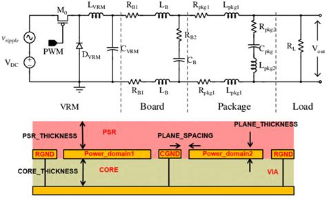
Lumped Element Modeling
Lumped element modeling is a technique used to represent the PDN as a network of discrete components such as resistors, inductors, and capacitors. It is a simplified approach that is suitable for low-frequency analysis.
The basic lumped element model of a PDN consists of the following components:
- Voltage Regulator Module (VRM): Represented as a voltage source with an output impedance.
- Bulk Capacitors: Used to provide low-frequency decoupling and reduce voltage ripple.
- Ceramic Capacitors: Used for high-frequency decoupling and reducing local impedance.
- Plane Capacitance: Represents the capacitance between power and ground planes.
- Trace Inductance: Represents the inductance of the interconnects.
Distributed Modeling
For high-frequency analysis, lumped element modeling becomes inaccurate due to the distributed nature of the PDN. In such cases, distributed modeling techniques are employed.
Distributed modeling involves representing the PDN as a network of transmission lines and lumped components. It takes into account the propagation delay, characteristic impedance, and attenuation of the interconnects.
Some common distributed modeling techniques include:
- 2D Transmission Line Modeling: Uses transmission line equations to model the power and ground planes as a 2D transmission line network.
- 3D Electromagnetic (EM) Modeling: Employs full-wave EM solvers to accurately simulate the PDN, considering the effects of vias, discontinuities, and coupling.

PDN Modeling in Schematic Design
PDN modeling begins at the schematic level, where the initial design decisions are made. The following steps are involved in PDN modeling during schematic design:
Component Selection
The first step is to select the appropriate components for the PDN. This includes:
- Voltage Regulator Module (VRM): Choose a VRM with suitable output voltage, current rating, and transient response.
- Bulk Capacitors: Select bulk capacitors with sufficient capacitance and low ESR (Equivalent Series Resistance) to provide low-frequency decoupling.
- Ceramic Capacitors: Choose ceramic capacitors with appropriate capacitance and voltage rating for high-frequency decoupling.
Decoupling Network Design
The decoupling network is designed to provide a low-impedance path for the high-frequency currents and minimize voltage fluctuations at the component power pins.
The decoupling network consists of ceramic capacitors placed close to the power pins of the components. The placement and values of the capacitors are determined based on the impedance target and the frequency range of interest.
Power Plane Partitioning
Power plane partitioning involves dividing the power plane into separate regions for different supply voltages or power domains. It helps in reducing noise coupling and improving power integrity.
During schematic design, the power plane partitioning strategy is defined, considering factors such as component placement, signal routing, and EMC requirements.

PDN Modeling in Layout Design
PDN modeling continues into the layout design phase, where the physical implementation of the PDN takes place. The following aspects are considered during PDN modeling in layout:
Power Plane Design
The power plane design involves creating a low-impedance, low-inductance power distribution network on the PCB. The key considerations in power plane design include:
- Plane Thickness: Thicker planes provide lower impedance and better current-carrying capacity.
- Plane Spacing: Adequate spacing between power and ground planes helps in reducing plane capacitance and improving high-frequency performance.
- Via Placement: Proper placement of vias is crucial for minimizing inductance and ensuring a low-impedance path for the supply current.
Decoupling Capacitor Placement
The placement of decoupling capacitors in the layout is critical for effective high-frequency decoupling. The guidelines for capacitor placement include:
- Place capacitors as close as possible to the power pins of the components.
- Use multiple vias to connect the capacitors to the power and ground planes to minimize inductance.
- Minimize the loop area formed by the capacitor and the vias to reduce the effective series inductance (ESL).
Power Routing
Power routing involves creating a low-impedance, low-inductance path for the supply current from the VRM to the components. The key considerations in power routing include:
- Use wide traces or copper pours to minimize resistance and inductance.
- Avoid long and thin traces that can introduce significant inductance.
- Use separate routing layers for power and ground to minimize coupling and crosstalk.
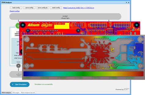
PDN Simulation and Verification
Once the PDN is modeled and implemented in the layout, simulation and verification are performed to assess its performance and identify any potential issues.
Frequency-Domain Simulation
Frequency-domain simulation involves analyzing the PDN impedance across a range of frequencies. It helps in identifying resonance peaks, evaluating the effectiveness of decoupling, and ensuring that the impedance target is met.
Tools such as S-parameter simulators or SPICE-based simulators are used for frequency-domain analysis. The simulation results are compared against the impedance target to verify the PDN performance.
Time-Domain Simulation
Time-domain simulation is used to analyze the transient behavior of the PDN, such as voltage droop and overshoot during load transitions. It helps in verifying the stability and dynamic performance of the PDN.
Tools such as SPICE simulators or transient solvers are used for time-domain analysis. The simulation results are compared against the specified voltage tolerances to ensure that the PDN can support the dynamic power requirements of the components.
Measurement and Validation
After the PDN is fabricated, measurements are performed to validate the simulation results and ensure that the PDN meets the desired performance criteria. Common measurement techniques include:
- Impedance Measurement: Using a vector network analyzer (VNA) or impedance analyzer to measure the PDN impedance across a range of frequencies.
- Voltage Ripple Measurement: Using an oscilloscope to measure the voltage ripple at the component power pins under different load conditions.
- Current Measurement: Using a current probe or a shunt resistor to measure the supply current and analyze the current distribution in the PDN.
The measurement results are compared against the simulation results and the specified requirements to validate the PDN design.
Best Practices for PDN Modeling
To ensure a robust and efficient PDN design, consider the following best practices:
- Start PDN modeling early in the design process to identify and address potential issues.
- Use accurate component models and simulation techniques to obtain reliable results.
- Collaborate with the layout team to ensure proper implementation of the PDN in the physical design.
- Perform thorough simulation and verification to assess the PDN performance across different operating conditions.
- Validate the PDN design through measurements and make necessary adjustments based on the results.
- Document the PDN design, including the component selection, decoupling strategy, and simulation results, for future reference and design reuse.
Conclusion
PDN modeling is a critical aspect of electronic design that ensures the power integrity and signal integrity of the system. By analyzing and optimizing the PDN impedance from schematic to layout, designers can mitigate issues such as voltage fluctuations, noise, and EMI.
This article provided an overview of PDN modeling techniques, including impedance analysis, lumped element modeling, distributed modeling, and simulation and verification methods. By following best practices and leveraging the right tools and techniques, designers can create robust and reliable PDNs that meet the power requirements of modern electronic systems.
Frequently Asked Questions (FAQ)
-
What is the purpose of PDN modeling?
PDN modeling aims to analyze and optimize the impedance characteristics of the power delivery system to ensure stable and reliable operation of the circuit. It helps in identifying and mitigating issues related to power integrity, signal integrity, and EMC. -
What are the key components of a PDN?
The key components of a PDN include the voltage regulator module (VRM), bulk capacitors, ceramic capacitors, power planes, and interconnects such as traces and vias. -
What is the difference between lumped element modeling and distributed modeling?
Lumped element modeling represents the PDN as a network of discrete components and is suitable for low-frequency analysis. Distributed modeling, on the other hand, considers the distributed nature of the PDN and is used for high-frequency analysis. It represents the PDN as a network of transmission lines and lumped components. -
How do you determine the impedance target for a PDN?
The impedance target is determined based on the power requirements of the components, the acceptable voltage ripple, and the target impedance of the voltage regulator module (VRM). It represents the maximum allowable impedance of the PDN at different frequencies. -
What are the key considerations in power plane design?
The key considerations in power plane design include plane thickness, plane spacing, and via placement. Thicker planes provide lower impedance, while adequate spacing between power and ground planes helps in reducing plane capacitance. Proper via placement is crucial for minimizing inductance and ensuring a low-impedance path for the supply current.
No responses yet