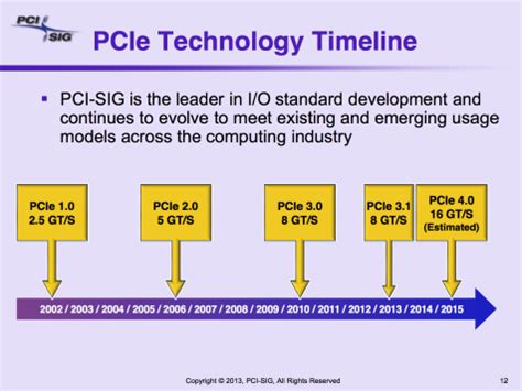
PCIe 5.0 Overview
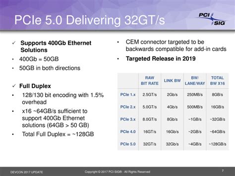
PCIe 5.0 maintains backwards compatibility with previous versions of PCIe while doubling the data rate to 32 GT/s per lane in each direction. This enables a x16 link to achieve a maximum theoretical bandwidth of 128 GB/s bi-directional. Key features of PCIe 5.0 include:
- 32 GT/s data rate per lane
- Backwards compatible with PCIe 4.0, 3.0, 2.0, and 1.x
- Support for x1, x2, x4, x8, x12, x16, and x32 link widths
- Extended tags and credits for improved protocol efficiency
- Precision Time Measurement for time synchronization
- Alternate protocol extension for user-defined protocols
The increased bandwidth of PCIe 5.0 enables new capabilities such as:
- 400 Gigabit Ethernet
- Next-generation GPUs and AI accelerators
- High-performance NVMe SSDs
- 200G InfiniBand interconnects
Signal Integrity Challenges
The 32 GT/s data rate of PCIe 5.0 introduces significant signal integrity challenges compared to previous generations. As the data rate increases, high-frequency losses in the transmission channel become more pronounced, leading to increased intersymbol interference (ISI) and reduced signal-to-noise ratio (SNR).
Key signal integrity challenges for PCIe 5.0 include:
Insertion Loss
Insertion loss is the reduction in signal power as it propagates through the channel, primarily due to dielectric loss and conductor loss. At 32 GT/s, the insertion loss at the Nyquist frequency (16 GHz) can exceed 30 dB for typical FR4 PCBs. This requires the use of advanced low-loss materials and equalization techniques.
Return Loss
Return loss is a measure of the amount of signal power reflected back to the transmitter due to impedance discontinuities in the channel. PCIe 5.0 specifies stringent return loss requirements to minimize reflections and ensure signal integrity.
| Return Loss Limits | Frequency |
|---|---|
| -8 dB | 100 MHz – 6 GHz |
| -7 dB | 6 GHz – 16 GHz |
| -6 dB | 16 GHz – 20 GHz |
Crosstalk
Crosstalk is the coupling of signal energy between adjacent PCIe lanes. At 32 GT/s, far-end crosstalk (FEXT) becomes a significant concern and can limit the maximum achievable link distance. Careful routing and shielding techniques must be used to minimize crosstalk.
Jitter
Jitter is the deviation of the signal edge from its ideal timing position. PCIe 5.0 has stringent jitter requirements to ensure proper data recovery and minimize bit errors.
| Jitter Component | Specification |
|---|---|
| Total Jitter (TJ) | 0.3 UI |
| Random Jitter (RJ) | 0.15 UI |
| Deterministic Jitter (DJ) | 0.15 UI |
Signal Integrity Analysis
Rigorous signal integrity analysis is essential to ensure that PCIe 5.0 designs meet the required specifications and operate reliably. Key aspects of PCIe 5.0 signal integrity analysis include:
Channel Modeling
Accurate modeling of the PCIe 5.0 channel is critical for predicting signal integrity and optimizing the design. The channel model should include:
- Transmission line geometry and materials
- Vias and connector models
- Package and die models
- Transmitter and receiver models
3D electromagnetic (EM) simulation tools can be used to extract S-parameters for the channel and create a complete end-to-end model.
Equalization
Equalization techniques are used to compensate for high-frequency losses in the channel and improve signal integrity. PCIe 5.0 uses a combination of transmitter and receiver equalization:
- Transmitter equalization:
- Feed-Forward Equalization (FFE)
- Pre-cursor and post-cursor taps
- Receiver equalization:
- Continuous Time Linear Equalization (CTLE)
- Decision Feedback Equalization (DFE)
Equalization parameters must be carefully optimized based on the specific channel characteristics to maximize the eye opening and minimize bit errors.
Bit Error Rate (BER) Simulation
BER simulation is used to predict the expected bit error rate of the PCIe 5.0 link based on the channel model and equalization settings. The goal is to achieve a BER of less than 1e-12 (one bit error per trillion bits) to ensure reliable operation.
BER simulation typically involves:
- Generating a long pseudo-random bit sequence (PRBS)
- Simulating the response of the equalized channel to the PRBS
- Comparing the received data to the transmitted data to count bit errors
- Extrapolating the BER to the desired confidence level
Advanced statistical techniques such as importance sampling can be used to efficiently estimate low BER values.
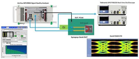
Measurement and Validation
Physical measurements are ultimately required to validate the signal integrity of the PCIe 5.0 design. Key measurements include:
- Eye diagrams
- Measure the eye opening at the receiver
- Verify sufficient margin to the eye mask
- Insertion loss
- Measure S21 magnitude
- Verify compliance with PCIe 5.0 IL limits
- Return loss
- Measure S11 magnitude
- Verify compliance with PCIe 5.0 RL limits
- Jitter
- Measure TJ, RJ, and DJ at the receiver
- Decompose jitter into its constituent components
- Verify compliance with PCIe 5.0 jitter limits
High-bandwidth oscilloscopes and vector network analyzers (VNAs) with low-noise receivers and advanced signal processing capabilities are required to accurately measure PCIe 5.0 signals.

PCIe 5.0 Design Considerations
To ensure signal integrity and reliable operation, PCIe 5.0 designs must carefully consider:
Material Selection
Low-loss PCB materials such as Megtron 6 or NELCO 4000-13 SI are recommended for PCIe 5.0 to minimize dielectric loss. The glass transition temperature (Tg) should be greater than 150°C to withstand lead-free solder reflow.
Via Design
High-aspect ratio vias with small diameters and short stub lengths are required to minimize via-related losses and reflections. Blind and buried vias are often used in PCIe 5.0 designs to optimize the signal path.
Connector Selection
PCIe 5.0 connectors must support 32 GT/s signaling with low loss and reflections. Compressible interface (CI) connectors with tightly controlled impedance and crosstalk are typically used.
Routing Constraints
Strict routing constraints must be followed to ensure signal integrity and minimize crosstalk:
- Matched length and symmetric routing for differential pairs
- Adequate spacing between adjacent pairs (5X trace width minimum)
- Minimize vias and layer transitions
- Avoid routing over gaps and slots in reference planes
- Route traces orthogonal to each other on adjacent layers
Shielding and Grounding
Proper shielding and grounding techniques are essential to minimize crosstalk and ensure signal integrity:
- Use ground vias to stitch reference planes together
- Maintain continuous reference planes under signal traces
- Use guard traces or coplanar waveguide structures for critical signals
- Implement ESD protection and EMI shielding
Frequently Asked Questions
What is the maximum length of a PCIe 5.0 link?
The maximum length of a PCIe 5.0 link depends on several factors, including the channel materials, equalization settings, and desired bit error rate. Typical maximum lengths are:
- 10-20 inches for server applications
- 5-10 inches for desktop applications
- 2-5 inches for mobile applications
Can PCIe 5.0 be used with copper cables?
Yes, PCIe 5.0 can be used with copper cables, but the maximum cable length is limited by the insertion loss of the cable. Active copper cables with built-in retimers can extend the reach to several meters.
What is the power consumption of PCIe 5.0?
PCIe 5.0 has a similar power consumption per lane as PCIe 4.0, but the total power scales with the increased number of lanes and bandwidth. A typical x16 PCIe 5.0 slot can consume up to 75 W.
How does PCIe 5.0 compare to other high-speed interfaces?
PCIe 5.0 offers similar bandwidth to other high-speed interfaces such as 100 Gbps Ethernet, InfiniBand HDR, and CCIX. However, PCIe has the advantage of being a widely adopted standard with a large ecosystem of devices and software support.
What tools are used for PCIe 5.0 signal integrity analysis?
PCIe 5.0 signal integrity analysis requires a combination of tools, including:
- 3D EM simulation tools (Ansys HFSS, Cadence Sigrity, Keysight ADS)
- Channel simulation tools (Keysight ADS, Cadence Sigrity SystemSI)
- Equalization and BER simulation tools (Keysight ADS, Cadence Sigrity SystemSI, Synopsys DesignWare)
- High-bandwidth oscilloscopes (Keysight UXR, Tektronix DPO7OE1)
- Vector network analyzers (Keysight PNA/PXI, Rohde & Schwarz ZNA)
By using these tools and following best design practices, engineers can ensure the signal integrity and reliable operation of PCIe 5.0 systems.
No responses yet