Introduction to Chiplet Interconnect Technology
The semiconductor industry has been pushing the boundaries of chip design and manufacturing to keep up with the ever-increasing demand for faster, more efficient, and cost-effective electronic devices. As the traditional method of creating monolithic integrated circuits (ICs) on a single die reaches its limits, the industry has been exploring alternative approaches to chip design and packaging. One such approach is the use of chiplets, which are smaller, specialized chips that can be interconnected to form a larger, more complex system.
Chiplet interconnect technology has emerged as a promising solution to the challenges faced by the semiconductor industry. By breaking down a large, complex chip into smaller, more manageable chiplets, designers can achieve higher yields, lower costs, and faster time-to-market. Additionally, chiplets allow for greater flexibility in chip design, as different chiplets can be optimized for specific functions and manufactured using different process technologies.
In this article, we will explore the differences between traditional printed circuit boards (PCBs), multichip modules (MCMs), chiplets, and the emerging silicon interconnect fabric technology. We will also discuss the advantages and challenges of each approach and provide insights into the future of chip design and packaging.
Traditional PCB-based Chip Packaging
Printed circuit boards (PCBs) have been the foundation of electronic device packaging for decades. A PCB is a flat board made of insulating material, such as fiberglass, with conductive pathways etched or printed onto its surface. These pathways, known as traces, connect various electronic components, such as ICs, resistors, and capacitors, to form a complete circuit.
PCBs offer several advantages, including:
- Low cost: PCBs are relatively inexpensive to manufacture, especially in large quantities.
- Ease of assembly: Components can be easily soldered onto a PCB using automated assembly processes.
- Reliability: PCBs have a long history of use and have proven to be reliable in a wide range of applications.
However, PCBs also have limitations, particularly when it comes to high-speed, high-density applications. As the demand for faster and more complex electronic devices grows, the limitations of PCBs become more apparent:
- Signal integrity: As the speed and frequency of signals increase, the traces on a PCB can introduce signal integrity issues, such as crosstalk and signal reflections.
- Density: PCBs have limited space for routing traces, which can restrict the number and complexity of components that can be placed on a single board.
- Thermal management: As the power density of electronic components increases, PCBs can struggle to dissipate heat effectively, leading to performance degradation and reliability issues.

Multichip Modules (MCMs)
To address some of the limitations of PCBs, the industry developed multichip modules (MCMs). An MCM is a specialized packaging technology that combines multiple ICs on a single substrate, such as ceramic or silicon. The ICs are interconnected using a variety of techniques, such as wire bonding, flip-chip bonding, or through-silicon vias (TSVs).
MCMs offer several advantages over traditional PCBs:
- Higher density: MCMs can accommodate a greater number of ICs in a smaller footprint, enabling more compact and efficient electronic devices.
- Improved signal integrity: By placing ICs closer together and using advanced interconnect technologies, MCMs can reduce signal integrity issues associated with longer traces on PCBs.
- Better thermal management: MCMs can be designed with advanced thermal management features, such as heat spreaders and cooling channels, to dissipate heat more effectively.
However, MCMs also have some drawbacks:
- Higher cost: MCMs are more expensive to manufacture than PCBs due to the specialized materials and processes involved.
- Limited flexibility: Once an MCM is designed and manufactured, it can be difficult to modify or upgrade without significant redesign and retooling.
- Yield issues: As the complexity of an MCM increases, the likelihood of manufacturing defects also increases, leading to lower yields and higher costs.

Chiplets and Chiplet Interconnect
Chiplets represent a new approach to chip design and packaging that aims to combine the benefits of MCMs with the flexibility and cost-effectiveness of smaller, specialized chips. A chiplet is a small, independent chip that is designed to perform a specific function, such as a CPU core, memory, or I/O interface. Multiple chiplets can be interconnected using advanced packaging technologies, such as silicon interposers or organic substrates, to form a complete system-on-chip (SoC).
The key advantages of chiplets and chiplet interconnect technology include:
- Yield improvement: By breaking down a large, complex chip into smaller chiplets, manufacturers can achieve higher yields and lower costs. If a defect occurs in one chiplet, only that chiplet needs to be discarded, rather than the entire chip.
- Design flexibility: Chiplets allow for greater flexibility in chip design, as different chiplets can be optimized for specific functions and manufactured using different process technologies. This enables designers to mix and match chiplets to create custom SoCs for specific applications.
- Faster time-to-market: By using pre-designed and pre-validated chiplets, designers can reduce the time and cost associated with developing and validating new chips.
- Improved performance: Chiplet interconnect technologies, such as silicon interposers and advanced packaging, can provide high-bandwidth, low-latency communication between chiplets, enabling better overall system performance.
However, chiplet interconnect technology also presents some challenges:
- Interconnect complexity: As the number of chiplets in a system increases, the complexity of the interconnect also increases. This can lead to signal integrity issues and higher power consumption.
- Thermal management: With multiple chiplets in close proximity, thermal management becomes more challenging. Advanced cooling solutions, such as liquid cooling or advanced heat spreaders, may be required to ensure reliable operation.
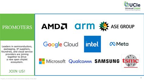
- Standards and ecosystem: The chiplet ecosystem is still emerging, and there is a lack of standardization in terms of chiplet interfaces and packaging technologies. This can lead to compatibility issues and higher costs for designers and manufacturers.

Silicon Interconnect Fabric
Silicon interconnect fabric (IF) is an emerging technology that aims to address some of the challenges associated with chiplet interconnect. A silicon IF is a high-density, high-bandwidth interconnect layer that is built using advanced semiconductor manufacturing processes, such as those used for creating transistors and other on-chip components.
The key advantages of silicon IF technology include:
- High bandwidth: Silicon IF can provide extremely high bandwidth communication between chiplets, with data rates exceeding 1 Tbps per link.
- Low latency: By using short, direct connections between chiplets, silicon IF can minimize signal latency and improve overall system performance.
- High density: Silicon IF can accommodate a large number of interconnects in a small area, enabling more compact and efficient chip packages.
- Compatibility with existing processes: Silicon IF can be manufactured using existing semiconductor manufacturing processes, reducing the cost and complexity of adoption.
However, silicon IF technology also faces some challenges:
- Power consumption: The high-speed, high-density nature of silicon IF can lead to higher power consumption compared to traditional interconnect technologies.
- Manufacturing complexity: Creating a silicon IF requires advanced manufacturing processes and precise alignment between chiplets, which can increase the complexity and cost of production.
- Thermal management: The high power density of silicon IF can exacerbate thermal management challenges, requiring advanced cooling solutions to ensure reliable operation.
Comparison Table
| Technology | Advantages | Disadvantages |
|---|---|---|
| PCB | – Low cost – Ease of assembly – Reliability |
– Limited signal integrity at high speeds – Limited density – Thermal management challenges |
| MCM | – Higher density – Improved signal integrity – Better thermal management |
– Higher cost – Limited flexibility – Yield issues |
| Chiplet Interconnect | – Yield improvement – Design flexibility – Faster time-to-market – Improved performance |
– Interconnect complexity – Thermal management challenges – Lack of standardization |
| Silicon IF | – High bandwidth – Low latency – High density – Compatibility with existing processes |
– Power consumption – Manufacturing complexity – Thermal management challenges |
Future Outlook and Conclusion
As the demand for faster, more efficient, and cost-effective electronic devices continues to grow, the semiconductor industry will need to continue innovating in chip design and packaging. Chiplet interconnect technology and silicon IF represent promising solutions to the challenges faced by traditional packaging approaches, such as PCBs and MCMs.
The adoption of chiplet interconnect and silicon IF will likely accelerate in the coming years, driven by the need for higher performance, lower costs, and faster time-to-market. However, the industry will need to address the challenges associated with these technologies, such as interconnect complexity, thermal management, and standardization.
In conclusion, the future of chip design and packaging lies in the continued development and refinement of advanced interconnect technologies, such as chiplet interconnect and silicon IF. By leveraging these technologies, the semiconductor industry can continue to push the boundaries of performance, efficiency, and cost-effectiveness, enabling the next generation of electronic devices and applications.
FAQ
-
What is a chiplet?
A chiplet is a small, independent chip that is designed to perform a specific function, such as a CPU core, memory, or I/O interface. Multiple chiplets can be interconnected using advanced packaging technologies to form a complete system-on-chip (SoC). -
What are the benefits of using chiplets?
Chiplets offer several benefits, including improved yield, design flexibility, faster time-to-market, and improved performance. By breaking down a large, complex chip into smaller chiplets, manufacturers can achieve higher yields and lower costs. Chiplets also allow for greater flexibility in chip design, as different chiplets can be optimized for specific functions and manufactured using different process technologies. -
What is silicon interconnect fabric (IF)?
Silicon interconnect fabric (IF) is an emerging technology that provides high-density, high-bandwidth interconnects between chiplets. It is built using advanced semiconductor manufacturing processes and can offer data rates exceeding 1 Tbps per link, low latency, and high density. -
What are the challenges associated with chiplet interconnect and silicon IF?
Some of the challenges associated with chiplet interconnect and silicon IF include interconnect complexity, thermal management, power consumption, manufacturing complexity, and lack of standardization. As the number of chiplets in a system increases, the complexity of the interconnect also increases, leading to signal integrity issues and higher power consumption. Thermal management also becomes more challenging with multiple chiplets in close proximity. -
What is the future outlook for chiplet interconnect and silicon IF technologies?
The adoption of chiplet interconnect and silicon IF technologies is expected to accelerate in the coming years, driven by the need for higher performance, lower costs, and faster time-to-market in the semiconductor industry. However, the industry will need to address the challenges associated with these technologies to ensure their widespread adoption and success.

No responses yet