What is PCBA Testing?
PCBA testing involves evaluating the functionality, reliability, and performance of an assembled printed circuit board. It is conducted to identify any defects, short circuits, open circuits, or component failures that may affect the overall operation of the electronic device. PCBA testing is essential to guarantee the quality and reliability of the final product.
Types of PCBA Tests
There are several types of PCBA tests that can be performed, depending on the specific requirements of the product and the manufacturing process. Let’s explore some of the most common types of PCBA tests:
- In-Circuit Testing (ICT):
In-Circuit Testing is a powerful technique that verifies the functionality of individual components on the PCBA. It involves using specialized test fixtures and probes to access the circuit nodes and perform measurements. ICT can detect issues such as: - Open circuits
- Short circuits
- Incorrect component values
- Missing components
- Incorrectly placed components
ICT is highly effective in identifying defects early in the manufacturing process, reducing the risk of faulty products reaching the end-users.
- Functional Testing:
Functional testing, also known as system-level testing, verifies the overall functionality of the PCBA as a complete unit. It ensures that the PCBA performs as intended and meets the specified requirements. Functional testing typically involves: - Powering up the PCBA
- Providing input signals
- Measuring output responses
- Verifying the expected behavior
Functional testing can be automated using test scripts and specialized equipment, allowing for efficient and repeatable testing.
- Boundary Scan Testing:
Boundary Scan Testing, also known as JTAG (Joint Test Action Group) testing, is a technique used to test the interconnections between integrated circuits (ICs) on a PCBA. It utilizes dedicated test access ports (TAPs) built into the ICs to access and control their inputs and outputs. Boundary Scan Testing enables: - Testing of complex PCBAs with high component density
- Detection of manufacturing defects such as open circuits, short circuits, and stuck-at faults
- Programming of on-board devices such as flash memories and FPGAs
Boundary Scan Testing is particularly useful for testing PCBAs with limited physical access to test points.
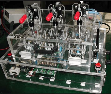
- Flying Probe Testing:
Flying Probe Testing is a non-contact testing method that uses movable test probes to access test points on the PCBA. The probes are guided by a computer-controlled system to perform electrical measurements at specific locations. Flying Probe Testing offers several advantages: - Flexibility in testing different PCBA designs without the need for custom test fixtures
- Ability to test both sides of the PCBA
- High test coverage, including hard-to-reach areas
- Reduced setup time compared to traditional test methods
Flying Probe Testing is commonly used for prototyping, low-volume production, and testing of complex PCBAs.
PCBA Test Coverage
To ensure comprehensive testing of a PCBA, it is important to consider the test coverage. Test coverage refers to the extent to which the PCBA is tested and the percentage of potential defects that can be detected. The goal is to achieve the highest possible test coverage while balancing the cost and time constraints.
| Test Type | Typical Test Coverage |
|---|---|
| In-Circuit Testing | 80-95% |
| Functional Testing | 60-80% |
| Boundary Scan Testing | 90-100% (limited to JTAG-enabled devices) |
| Flying Probe Testing | 80-95% |
It is worth noting that achieving 100% test coverage is often impractical due to the complexity of modern PCBAs and the limitations of testing methods. However, by combining multiple testing techniques and carefully designing the test strategy, manufacturers can achieve a high level of confidence in the quality and reliability of the PCBAs.
Best Practices for PCBA Testing
To ensure effective and efficient PCBA testing, here are some best practices to follow:
1. Design for Testability (DFT)
Design for Testability (DFT) is an approach that involves incorporating testability features into the PCBA design from the early stages. DFT techniques include:
– Adding test points and test pads for easy access during testing
– Utilizing boundary scan-compatible components
– Providing clear and accurate documentation, including schematics and bill of materials (BOM)
By considering testability during the design phase, manufacturers can streamline the testing process and improve the overall quality of the PCBA.
2. Develop a Comprehensive Test Plan
A well-defined test plan is crucial for effective PCBA testing. The test plan should outline the specific tests to be performed, the test sequence, the acceptance criteria, and the resources required. It should also consider the following aspects:
– Test coverage and test point accessibility
– Test equipment and software requirements
– Test fixture design and fabrication
– Test program development and debugging
– Test data analysis and reporting
A comprehensive test plan ensures that all necessary tests are performed and helps in identifying potential issues early in the testing process.
3. Implement Automated Testing
Automated testing can significantly improve the efficiency and accuracy of PCBA testing. By using automated test equipment (ATE) and software tools, manufacturers can:
– Reduce human errors and inconsistencies
– Increase test speed and throughput
– Generate detailed test reports and data analysis
– Enable remote monitoring and control of the testing process
Automated testing is particularly beneficial for high-volume production and repetitive testing tasks.
4. Perform Regular Maintenance and Calibration
To ensure the accuracy and reliability of PCBA testing, it is essential to perform regular maintenance and calibration of the test equipment. This includes:
– Cleaning and inspecting test fixtures and probes
– Verifying the accuracy of measurement instruments
– Updating software and firmware to the latest versions
– Performing periodic calibration of test equipment
Regular maintenance and calibration help in preventing test errors and ensuring consistent test results over time.
5. Foster Collaboration and Communication
Effective PCBA testing requires collaboration and communication among various teams, including design, manufacturing, and quality assurance. Fostering a culture of open communication and teamwork can help in:
– Identifying and resolving issues quickly
– Sharing knowledge and best practices
– Continuously improving the testing process
– Ensuring alignment with customer requirements and expectations
Regular meetings, cross-functional teams, and clear documentation can facilitate collaboration and communication throughout the PCBA testing process.

Frequently Asked Questions (FAQ)
-
What is the difference between ICT and functional testing?
In-Circuit Testing (ICT) focuses on testing individual components and their interconnections on the PCBA, while functional testing verifies the overall functionality of the assembled PCBA as a complete unit. ICT is performed at the component level, whereas functional testing is done at the system level. -
How long does PCBA testing typically take?
The duration of PCBA testing depends on various factors, such as the complexity of the PCBA, the number of components, the testing methods used, and the test coverage required. Simple PCBAs may take a few minutes to test, while complex boards with high component counts can take several hours. The specific testing time should be determined based on the test plan and the manufacturing requirements. -
Can PCBA testing guarantee 100% defect-free products?
While PCBA testing aims to identify and eliminate defects, achieving 100% defect-free products is practically impossible. There is always a small chance of defects escaping detection during testing. However, by implementing comprehensive testing strategies, following best practices, and continuously improving the testing process, manufacturers can minimize the risk of defective products reaching the end-users. -
How often should test equipment be calibrated?
The frequency of test equipment calibration depends on the manufacturer’s recommendations, industry standards, and the specific requirements of the PCBA being tested. Typically, test equipment should be calibrated at least once a year or as specified by the manufacturer. More frequent calibration may be necessary for critical measurements or high-precision applications. -
What is the role of test coverage in PCBA testing?
Test coverage refers to the extent to which the PCBA is tested and the percentage of potential defects that can be detected. Higher test coverage means a greater chance of identifying defects and ensuring the quality of the PCBA. However, achieving 100% test coverage is often impractical due to the complexity of modern PCBAs and the limitations of testing methods. The goal is to strike a balance between test coverage and the cost and time constraints of the manufacturing process.

Conclusion
PCBA testing is a vital step in ensuring the quality, reliability, and functionality of electronic devices. By understanding the various types of PCBA tests, implementing best practices, and following a comprehensive test plan, manufacturers can effectively identify and eliminate defects, reducing the risk of faulty products reaching the end-users.
As technology continues to advance and PCBAs become more complex, the importance of PCBA testing will only grow. By staying up-to-date with the latest testing techniques, investing in automated testing solutions, and fostering a culture of continuous improvement, manufacturers can meet the ever-increasing demands for high-quality electronic products in today’s competitive market.

No responses yet