What is PCB Assembly (PCBA)?
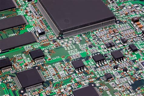
PCB Assembly (PCBA) is the process of attaching electronic components to a printed circuit board (PCB) to create a functional electronic device. The PCB serves as the foundation for the electronic components, providing the necessary electrical connections and mechanical support. The assembly process involves soldering components onto the PCB, ensuring proper placement and connection to create a complete and functional electronic circuit.
The PCB Assembly Process
The PCBA process typically involves the following steps:
-
Solder Paste Application: Solder paste, a mixture of tiny solder particles suspended in flux, is applied to the PCB’s pads where the components will be placed. This is usually done using a stencil or screen printing process to ensure precise and consistent application.
-
Component Placement: Electronic components, such as resistors, capacitors, integrated circuits (ICs), and connectors, are placed onto the PCB’s surface. This can be done manually for small-scale production or using automated pick-and-place machines for larger volumes. The machines use computer-aided design (CAD) data to accurately place the components on the board.
-
Reflow Soldering: The PCB with the placed components is then subjected to a reflow soldering process. The board is heated in a reflow oven, causing the solder paste to melt and form a permanent electrical and mechanical connection between the components and the PCB pads. The temperature profile is carefully controlled to ensure proper solder joint formation and to avoid damage to the components.
-
Inspection and Testing: After the reflow soldering process, the assembled PCB undergoes visual inspection and automated optical inspection (AOI) to check for any defects, such as missing components, incorrect placement, or solder bridging. Electrical testing, such as in-circuit testing (ICT) or functional testing, may also be performed to ensure the PCBA functions as intended.
-
Cleaning and Coating: If required, the PCBA may undergo cleaning to remove any residual flux or contaminants. Additionally, conformal coating or potting may be applied to protect the PCBA from environmental factors like moisture, dust, or vibration.
-
Final Assembly and Packaging: The tested and approved PCBA is then integrated into the final product or enclosure. This may involve additional steps such as wiring, mounting, and packaging, depending on the specific application and product requirements.
Advantages of PCB Assembly
PCBA offers several advantages over traditional point-to-point wiring or breadboard prototyping:
-
Compact and Efficient Design: PCBs allow for a compact and efficient layout of electronic components, minimizing the overall size of the device and improving its performance. The use of multi-layer PCBs further enhances the design flexibility and component density.
-
Reliability and Durability: Properly assembled PCBAs provide a reliable and durable solution for electronic devices. The soldered connections are strong and resistant to vibration, shock, and thermal stresses, ensuring long-term performance and reliability.
-
Mass Production Capability: PCBA enables mass production of electronic devices by automating the assembly process. Automated pick-and-place machines and reflow soldering ovens allow for high-volume production with consistent quality and reduced manufacturing time.
-
Cost-Effectiveness: PCB assembly offers cost savings compared to traditional wiring methods, especially for high-volume production. The use of automated processes and standardized components reduces labor costs and minimizes human errors, resulting in a more cost-effective manufacturing process.
-
Design Flexibility: PCBs offer design flexibility by allowing for the integration of various components and technologies, such as surface mount devices (SMDs), through-hole components, and advanced packaging techniques. This enables the creation of complex and sophisticated electronic devices.

Types of PCB Assembly
There are two main types of PCB assembly based on the component mounting method:
-
Surface Mount Technology (SMT) Assembly: SMT assembly involves placing and soldering components directly onto the surface of the PCB. SMT components, such as chip resistors, chip capacitors, and small outline integrated circuits (SOICs), have small leads or terminations that are soldered to pads on the PCB surface. SMT assembly allows for higher component density, smaller board sizes, and improved high-frequency performance compared to through-hole assembly.
-
Through-Hole (TH) Assembly: TH assembly involves inserting component leads through holes drilled in the PCB and soldering them to pads on the opposite side of the board. TH components, such as axial lead resistors, radial lead capacitors, and dual in-line package (DIP) ICs, have longer leads that are inserted into the holes. TH assembly is often used for components that require higher mechanical strength or for devices that need to withstand higher power dissipation.
In many cases, a combination of SMT and TH assembly, known as mixed technology assembly, is used in PCBAs to accommodate different component types and design requirements.
PCBA Quality Control and Testing
Ensuring the quality and reliability of PCBAs is crucial for the proper functioning and longevity of electronic devices. Quality control and testing are integral parts of the PCBA process. Some common quality control and testing methods include:
-
Visual Inspection: Visual inspection is the first line of defense in detecting assembly defects. Trained operators or automated optical inspection (AOI) systems check for visible defects such as missing components, misaligned parts, solder bridges, or insufficient solder joints.
-
X-Ray Inspection: X-ray inspection is used to examine solder joints and component placement that are not visible from the surface, such as ball grid array (BGA) packages or hidden connections. X-ray systems can detect voids, cracks, or other defects in solder joints.
-
In-Circuit Testing (ICT): ICT is an automated testing method that verifies the presence, orientation, and value of components on the PCBA. It uses a bed-of-nails fixture to make contact with specific test points on the board and performs electrical measurements to ensure the correct functioning of individual components and circuits.
-
Functional Testing: Functional testing involves powering up the PCBA and testing its overall functionality and performance. It checks whether the PCBA operates as intended and meets the specified requirements. Functional testing may include tests for power consumption, signal integrity, communication interfaces, and software functionality.
-
Boundary Scan Testing: Boundary scan testing, also known as JTAG testing, is a method for testing the interconnections between integrated circuits (ICs) on a PCBA. It uses a serial data path to access and control the I/O pins of the ICs, enabling the detection of shorts, opens, and other connectivity issues.
-
Environmental Testing: Environmental testing exposes the PCBA to various environmental conditions, such as temperature extremes, humidity, vibration, or shock, to assess its durability and reliability under real-world operating conditions. This helps identify potential weaknesses or failure modes.
| Testing Method | Purpose |
|---|---|
| Visual Inspection | Detect visible defects (missing components, solder bridges) |
| X-Ray Inspection | Examine hidden solder joints and component placement |
| In-Circuit Testing | Verify presence, orientation, and value of components |
| Functional Testing | Check overall functionality and performance |
| Boundary Scan Testing | Test interconnections between integrated circuits |
| Environmental Testing | Assess durability and reliability under real-world conditions |
By implementing comprehensive quality control and testing procedures, manufacturers can identify and address defects early in the production process, reducing rework, improving yield, and ensuring the delivery of high-quality and reliable PCBAs.

Frequently Asked Questions (FAQ)
- What is the difference between PCB and PCBA?
-
A PCB (printed circuit board) is the bare board without any components mounted on it. It consists of conductive tracks, pads, and other features etched from copper sheets laminated onto a non-conductive substrate. On the other hand, PCBA (PCB assembly) refers to the process of assembling electronic components onto the PCB to create a functional electronic circuit.
-
What are the common components used in PCBA?
-
Common components used in PCBA include resistors, capacitors, inductors, diodes, transistors, integrated circuits (ICs), connectors, switches, and various types of sensors. These components are available in different packages, such as surface mount devices (SMDs) and through-hole components, depending on the assembly method and design requirements.
-
What is the purpose of solder paste in PCBA?
-
Solder paste is a critical material used in the PCBA process, particularly for surface mount technology (SMT) assembly. It serves two main purposes: providing a temporary adhesive to hold the components in place during the assembly process and forming a permanent electrical and mechanical connection between the components and the PCB pads after the reflow soldering process.
-
How is the quality of PCBA ensured?
-
Quality control and testing are integral parts of the PCBA process to ensure the quality and reliability of the assembled boards. Various methods are employed, including visual inspection, automated optical inspection (AOI), X-ray inspection, in-circuit testing (ICT), functional testing, boundary scan testing, and environmental testing. These methods help identify and address defects, ensure proper functionality, and assess the durability and reliability of the PCBA.
-
What are the advantages of using automated assembly processes in PCBA?
- Automated assembly processes, such as pick-and-place machines and reflow soldering ovens, offer several advantages in PCBA. They enable high-volume production with consistent quality, reduce manufacturing time, minimize human errors, and provide cost-effectiveness compared to manual assembly methods. Automated processes also allow for precise component placement and uniform solder joint formation, resulting in improved reliability and performance of the assembled boards.
In conclusion, PCBA is a critical process in the manufacturing of electronic devices, combining PCBs with electronic components to create functional circuits. By understanding the PCBA process, its advantages, types, and quality control methods, designers and manufacturers can create reliable, efficient, and cost-effective electronic products. As technology advances and the demand for electronic devices continues to grow, PCBA will remain a vital aspect of the electronics industry, enabling the development of innovative and high-performance products.
No responses yet