Introduction to PCB Vias
Printed Circuit Boards (PCBs) are essential components in modern electronics. They provide a platform for mounting and interconnecting electronic components to create functional circuits. One crucial element in PCB design is the via, which enables electrical connections between different layers of a multi-layer PCB. In this article, we will dive deep into the world of PCB vias, exploring their types, applications, and factors to consider when choosing the right via for your PCB design.
What is a PCB Via?
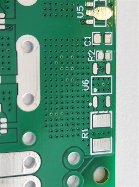
A PCB via is a small hole drilled through a printed circuit board to create an electrical connection between different layers of the board. Vias are typically plated with a conductive material, such as copper, to ensure reliable electrical conductivity. They allow signals and power to pass through the layers of the PCB, enabling more complex and compact circuit designs.
The Role of Vias in PCB Design
Vias play a crucial role in PCB design by:
- Interconnecting different layers of a multi-layer PCB
- Providing a means for signal routing and power distribution
- Enabling more compact and efficient PCB layouts
- Facilitating heat dissipation and grounding

Types of PCB Vias
There are several types of PCB vias, each with its own characteristics and applications. Let’s explore the most common types:
Through-Hole Vias
Through-hole vias are the most basic and widely used type of via. They are drilled through the entire thickness of the PCB and are plated with a conductive material. Through-hole vias offer strong mechanical stability and are suitable for high-current applications. However, they consume more board space compared to other via types.
Blind Vias
Blind vias are drilled from one side of the PCB and terminate at a specific inner layer without passing through the entire board thickness. They are used to connect an outer layer to one or more inner layers. Blind vias offer improved space utilization and allow for more compact PCB designs. However, they are more expensive to manufacture compared to through-hole vias.
Buried Vias
Buried vias are located entirely within the inner layers of a PCB and do not extend to either surface of the board. They are used to interconnect inner layers without consuming space on the outer layers. Buried vias enable more complex routing and higher component density. However, they are the most expensive type of via to manufacture.
Microvias
Microvias are small-diameter vias, typically less than 150 microns in diameter. They are used in high-density interconnect (HDI) PCBs to achieve fine-pitch connections and high-density routing. Microvias can be formed using various methods, such as laser drilling or photolithography. They offer improved signal integrity and reduced signal delay. However, they require advanced manufacturing processes and are more expensive compared to larger vias.
Stacked Vias
Stacked vias are formed by aligning and interconnecting multiple vias on different layers of the PCB. They are used to create connections between non-adjacent layers, allowing for more efficient use of board space. Stacked vias can be a combination of through-hole, blind, or buried vias. They offer flexibility in routing and enable more complex PCB designs.

Factors to Consider When Choosing PCB Vias
When selecting the appropriate via type for your PCB design, consider the following factors:
-
PCB Layer Count: The number of layers in your PCB will influence the choice of via type. Through-hole vias are suitable for simple 2-layer boards, while blind and buried vias are used in multi-layer PCBs to optimize space utilization.
-
Signal Integrity: Consider the signal integrity requirements of your design. Microvias offer improved signal integrity and reduced signal delay, making them suitable for high-speed applications. Through-hole vias, on the other hand, may introduce signal reflections and crosstalk.
-
Current Carrying Capacity: If your design requires high current carrying capacity, through-hole vias are a good choice due to their larger cross-sectional area. Microvias and smaller vias may have limitations in handling high currents.
-
Manufacturing Cost: Different via types have varying manufacturing costs. Through-hole vias are the most cost-effective, while blind, buried, and microvias require more advanced manufacturing processes and are more expensive. Consider your budget and production volume when selecting the via type.
-
Board Space Constraints: If board space is limited, consider using blind, buried, or microvias to optimize space utilization. These via types allow for more compact routing and higher component density compared to through-hole vias.
-
Reliability and Durability: Consider the reliability and durability requirements of your PCB. Through-hole vias offer strong mechanical stability, making them suitable for applications with high mechanical stress. Microvias and smaller vias may be more susceptible to thermal and mechanical stress.

PCB Via Design Considerations
When designing vias for your PCB, keep the following considerations in mind:
-
Via Size: Choose an appropriate via size based on the current carrying requirements, signal integrity, and manufacturing capabilities. Larger vias can handle higher currents but consume more board space, while smaller vias offer space savings but have limitations in current handling.
-
Via Spacing: Ensure sufficient spacing between vias to prevent signal interference and manufacturing issues. Follow the design rules and guidelines provided by your PCB manufacturer to maintain proper via spacing.
-
Pad Size: Select an appropriate pad size for your vias based on the drilling and plating requirements. The pad size should be large enough to accommodate the via hole and provide sufficient annular ring for reliable connections.
-
Via Filling: Consider filling vias with non-conductive materials, such as epoxy or resin, to improve mechanical stability, prevent solder wicking, and enhance thermal dissipation. Via filling is commonly used in high-reliability applications.
-
Thermal Management: Vias can also be used for thermal management by providing a path for heat dissipation. Thermal vias are strategically placed near heat-generating components to conduct heat away from the components and into the PCB substrate or heatsinks.
Frequently Asked Questions (FAQ)
1. What is the difference between a through-hole via and a blind via?
A through-hole via passes through the entire thickness of the PCB, while a blind via starts from one surface and terminates at an inner layer without reaching the opposite surface.
2. Can I use microvias in a 2-layer PCB?
While microvias are commonly used in multi-layer HDI PCBs, they can also be used in 2-layer PCBs for specific applications that require fine-pitch connections or high-density routing.
3. How do I determine the appropriate via size for my PCB design?
The appropriate via size depends on factors such as current carrying requirements, signal integrity, and manufacturing capabilities. Consult with your PCB manufacturer and follow their design guidelines to determine the suitable via size for your specific design.
4. Are buried vias more expensive than through-hole vias?
Yes, buried vias are generally more expensive to manufacture compared to through-hole vias because they require additional processing steps and precise alignment between layers.
5. Can vias be used for grounding purposes?
Yes, vias can be used for grounding by connecting ground planes on different layers of the PCB. This helps to create a low-impedance path for return currents and improves signal integrity.
Conclusion
PCB vias are essential elements in PCB design, enabling electrical connections between different layers of a multi-layer board. Understanding the types of vias, their characteristics, and their applications is crucial for creating efficient and reliable PCB designs. When choosing the appropriate via type, consider factors such as PCB layer count, signal integrity, current carrying capacity, manufacturing cost, board space constraints, and reliability requirements.
By carefully selecting and designing vias for your PCB, you can optimize signal routing, power distribution, and overall circuit performance. As PCB technology continues to advance, staying informed about the latest via technologies and design techniques will help you create cutting-edge electronics that meet the demands of modern applications.
| Via Type | Description | Applications |
|---|---|---|
| Through-Hole Via | Drilled through the entire PCB thickness | Simple 2-layer PCBs, high-current applications |
| Blind Via | Connects an outer layer to inner layers | Multi-layer PCBs, space optimization |
| Buried Via | Located entirely within inner layers | Multi-layer PCBs, complex routing |
| Microvia | Small-diameter via (< 150 microns) | HDI PCBs, fine-pitch connections |
| Stacked Via | Interconnects multiple vias on different layers | Non-adjacent layer connections, efficient space utilization |
As you embark on your PCB design journey, keep these via types and considerations in mind to create robust and efficient printed circuit boards that power the electronic devices of tomorrow.
No responses yet