What are PCB Vias?
PCB vias are small holes drilled into a printed circuit board (PCB) that allow signals to pass from one layer of the board to another. Vias are an essential part of multi-layer PCB design, enabling complex routing schemes and more compact board layouts. Without vias, PCBs would be limited to just single-sided or double-sided designs.
Vias come in several different types, each with their own characteristics and best use cases. Choosing the right type of via is important for ensuring optimal electrical performance, manufacturability, reliability, and cost-effectiveness of the PCB.
In this comprehensive guide, we’ll dive deep into the world of PCB vias. You’ll learn:
- The different types of PCB vias and their definitions
- How each via type is manufactured
- The advantages and disadvantages of each via type
- Design considerations and use cases for selecting via types
- Answers to frequently asked questions about PCB vias
By the end, you’ll have a solid understanding of everything related to vias for printed circuit boards. Let’s get started!
Types of PCB Vias
Here are the main types of vias used in PCB design and manufacturing:
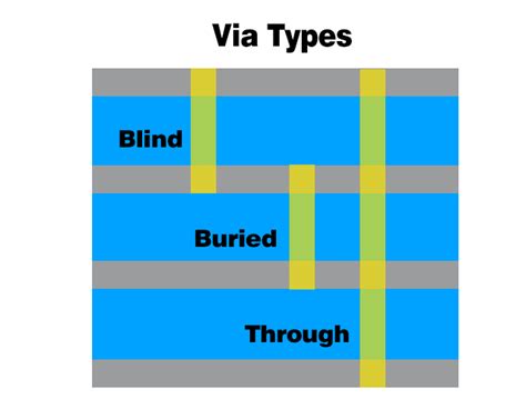
Through-Hole Vias
Through-hole vias are the most basic and common type. They consist of a hole that is drilled completely through the PCB, from the top layer to the bottom layer. The hole walls are then plated with a conductive material, usually copper, to create an electrical connection between the layers.
Advantages:
- Strong mechanical connection
- Allows through-hole component leads to be soldered
- Reliable electrical connection
- Easiest and cheapest to manufacture
Disadvantages:
- Consumes a lot of board space
- Limits routing density on inner layers
- Not suitable for high-density designs
Best Uses:
- Boards with through-hole components
- Simple double-sided boards
- Low-cost applications
- Prototypes and small quantities
Blind Vias
Blind vias are holes drilled from either the top or bottom surface of the PCB, but they do not go all the way through the board. Instead, they stop and terminate at an inner layer. Blind vias are more complex and expensive to manufacture than through-hole vias.
Advantages:
- Saves board space
- Allows higher routing density
- Provides direct connection to inner layers
- Shorter signal paths than through-hole
Disadvantages:
- More expensive to fabricate
- Requires sequential lamination process
- Limited layer accessibility
- Harder to inspect and test
Best Uses:
- High-density designs
- Controlled impedance routing
- RF and high-speed applications
- Connecting SMT components to inner planes
Buried Vias
Buried vias are holes that are drilled into the inner layers of the PCB, but do not extend to either the top or bottom surface of the finished board. The hole is plated to connect the inner layers. Buried vias offer many of the same benefits as blind vias in terms of saving space and enabling dense routing.
Advantages:
- Provides highest routing density
- Keeps all vias within inner layers
- Allows stacking multiple via types
- Ideal for space-constrained designs
Disadvantages:
- Requires sequential lamination
- Most complex and expensive via type
- Cannot be accessed for probing or rework
- Difficult to inspect buried connections
Best Uses:
- Very high density PCBs
- Boards with 6 or more layers
- HDI and advanced packaging substrates
- Medical, aerospace, and defense applications
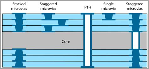
Micro Vias
Micro vias are a special type of blind via with a very small diameter, typically less than 150 microns. They are commonly used in high-density interconnect (HDI) PCB designs to create super-fine pitch connections between the outer layer and the first inner layer.
Advantages:
- Extremely small size (< 150 μm)
- Enables very fine-pitch BGAs and CSPs
- High routing density on outer layers
- Shorter signal paths and lower inductance
Disadvantages:
- Requires laser drilling or special processes
- Limited to 1-2 layers in depth
- Micro via in pad may cause assembly issues
- Requires strict design rules and tolerances
Best Uses:
- HDI and advanced IC Packaging
- Mobile and consumer electronics
- Mini/micro BGAs and CSPs
- Wearables and IoT devices
Via Manufacturing Processes
The different types of vias are created using various manufacturing processes during PCB fabrication. Here’s an overview of the common methods:
Mechanical Drilling
- Used for through-hole vias
- CNC drill bit creates holes through all layers
- Hole sizes typically > 200 μm
Laser Drilling
- Used for blind and buried vias
- CO2 or UV laser vaporizes hole through selected layers
- Allows smaller holes down to 25 μm
Photo Via
- Used for blind vias
- Photoimageable dielectric is exposed and developed
- Allows via creation on outer layers
Plasma Etching
- Used for blind and buried vias
- Plasma gas removes dielectric material
- Enables high aspect ratio vias
Conductive Paste Filling
- Used to fill blind and buried vias
- Screen printing deposits conductive paste into holes
- Provides structural support and thermal management

Via Design Considerations
When designing a PCB, there are several key factors to consider when selecting and using vias:
Aspect Ratio
- Ratio of via depth to diameter
- Higher aspect ratios are more difficult to manufacture reliably
- Typical ratios are 6:1 to 10:1 depending on via type and process
Pad Size and Via Pitch
- Pad size determines minimum via pitch (center-to-center spacing)
- Smaller pads allow tighter pitches but may impact reliability
- Consult with manufacturer for recommended pad/pitch dimensions
Via Stackup
- Determines which layers vias can connect to
- Influenced by number of layers, drilling sequence, and lamination cycles
- Must consider signal integrity and EMI effects of via stubs
Thermal Reliability
- Vias can act as heat sinks to inner planes
- Too many vias can cause localized heating and thermal stress
- Filled vias help with heat transfer but may induce stresses
Signal Integrity
- Vias can affect impedance matching, crosstalk, and losses
- Stub length should be minimized, especially at high frequencies
- Ground vias and stitching help with shielding and current return paths
FAQ About PCB Vias
Q: What is the difference between a via and a pad?
A: A pad is a flat, typically circular, conductive area on the surface of a PCB used for soldering components or creating test points. A via is a hole that passes through multiple layers of the PCB to connect different pads and traces on different layers together.
Q: Can vias be filled with non-conductive material?
A: Yes, vias can be filled with a non-conductive epoxy resin to provide structural support, improve thermal transfer, and prevent contamination. However, non-conductive filling does not create an electrical connection between layers.
Q: What is via in pad technology?
A: Via in pad (VIP) is a technique where a micro via is placed directly within a surface mount pad, usually to connect to the first inner layer. This allows for higher density routing and can be used with fine-pitch BGAs and CSPs. However, VIP requires careful design and assembly considerations.
Q: How do buried and blind vias affect PCB assembly?
A: Since buried vias are completely internal to the PCB, they do not have a direct impact on assembly. Blind vias that extend to the outer surface can be used for connecting surface mount components, but may require special consideration for solder paste application and reflow profiles.
Q: What is a via stub and why is it important?
A: A via stub is the unused portion of a through-hole via that extends beyond the layers it is connecting. Via stubs can cause signal integrity issues, especially at high frequencies, by creating impedance mismatches and reflections. Techniques like back-drilling or blind/buried vias can be used to minimize stub length.
Conclusion
Vias are a critical element of PCB design that enable the creation of multi-layer boards with complex routing schemes. By understanding the different types of vias, their manufacturing processes, and key design considerations, PCB designers can make informed decisions about how to optimize their board layouts for electrical performance, manufacturability, and cost.
While through-hole vias remain the most common and economical choice for many applications, blind, buried, and micro vias offer significant advantages in terms of routing density, signal integrity, and package size reduction. As electronic devices continue to get smaller and more complex, the use of advanced via technologies will become increasingly important.
When designing a PCB, it’s essential to work closely with your fabrication partner to ensure that your via choices are compatible with their manufacturing capabilities and design rules. By following best practices and leveraging the right via types for your application, you can create reliable, high-performance PCBs that meet the demands of today’s electronic products.
No responses yet