Introduction to PCB Transmission Lines
Printed Circuit Boards (PCBs) are essential components in modern electronic devices, enabling the interconnection of various components and facilitating signal transmission. As the demand for high-speed and high-frequency applications continues to grow, understanding the principles of PCB transmission lines becomes increasingly important. This article delves into the fundamentals of PCB transmission lines, their characteristics, and design considerations to ensure optimal signal integrity and system performance.
What are PCB Transmission Lines?
PCB transmission lines are conductive traces on a printed circuit board that are designed to carry electrical signals between components. These traces are specifically engineered to maintain the integrity of the signal as it propagates through the board. Transmission lines are crucial in high-speed and high-frequency applications, where signal integrity is of utmost importance.
Types of PCB Transmission Lines
There are several types of PCB transmission lines, each with its own characteristics and applications. The most common types include:
-
Microstrip: Microstrip transmission lines consist of a conductive trace on the top layer of the PCB, with a ground plane on the bottom layer. They are widely used in high-frequency applications due to their simplicity and ease of fabrication.
-
Stripline: Stripline transmission lines are embedded within the PCB, sandwiched between two ground planes. They offer better shielding and reduced electromagnetic interference compared to microstrip lines.
-
Coplanar Waveguide (CPW): CPW transmission lines have a conductive trace with ground planes on either side, all on the same layer of the PCB. They provide good signal isolation and are suitable for high-frequency applications.
-
Differential Pairs: Differential pair transmission lines consist of two parallel traces that carry differential signals. They are commonly used in high-speed digital interfaces, such as USB, HDMI, and PCIe, to reduce electromagnetic interference and improve signal integrity.
Characteristics of PCB Transmission Lines
To effectively design and optimize PCB transmission lines, it is essential to understand their key characteristics. These characteristics determine the behavior of the signal as it propagates through the transmission line.
Characteristic Impedance
Characteristic impedance is a critical parameter of PCB transmission lines. It is the ratio of the voltage to the current in a transmission line when the line is infinitely long or terminated with its characteristic impedance. The characteristic impedance depends on the geometry of the transmission line, the dielectric constant of the PCB material, and the frequency of the signal.
The characteristic impedance of a transmission line is given by the following equation:
Z₀ = √(L/C)
Where:
– Z₀ is the characteristic impedance
– L is the inductance per unit length
– C is the capacitance per unit length
Maintaining a consistent characteristic impedance throughout the transmission line is crucial for minimizing reflections and ensuring proper signal propagation.
Propagation Delay
Propagation delay refers to the time it takes for a signal to travel from one end of the transmission line to the other. It is determined by the physical length of the transmission line and the velocity of propagation, which depends on the dielectric constant of the PCB material.
The propagation delay can be calculated using the following equation:
t_d = l / v_p
Where:
– t_d is the propagation delay
– l is the length of the transmission line
– v_p is the velocity of propagation
Minimizing propagation delay is important in high-speed applications to ensure proper timing and synchronization between components.
Attenuation
Attenuation is the loss of signal strength as it propagates through the transmission line. It is caused by various factors, including conductor losses, dielectric losses, and radiation losses. Attenuation increases with frequency and can limit the maximum length of the transmission line.
The attenuation constant (α) of a transmission line is given by:
α = (R/2Z₀) + (GZ₀/2)
Where:
– α is the attenuation constant
– R is the series resistance per unit length
– G is the shunt conductance per unit length
– Z₀ is the characteristic impedance
Minimizing attenuation is crucial for maintaining signal integrity over longer distances and at higher frequencies.

PCB Transmission Line Design Considerations
Designing PCB transmission lines requires careful consideration of various factors to ensure optimal signal integrity and system performance. Some key design considerations include:
Impedance Matching
Impedance matching is the process of ensuring that the characteristic impedance of the transmission line matches the impedance of the source and load. Proper impedance matching minimizes reflections and maximizes power transfer. Common impedance values for PCB transmission lines include 50Ω, 75Ω, and 100Ω.
Trace Width and Spacing
The width and spacing of the transmission line traces play a crucial role in determining the characteristic impedance and signal integrity. Wider traces have lower impedance and can carry more current, while narrower traces have higher impedance and are more susceptible to noise. The spacing between traces affects the coupling and crosstalk between adjacent signals.
| Impedance (Ω) | Trace Width (mm) | Trace Spacing (mm) |
|---|---|---|
| 50 | 0.25 | 0.20 |
| 75 | 0.15 | 0.30 |
| 100 | 0.10 | 0.40 |
Table 1: Example trace width and spacing values for different impedances
Termination Techniques
Termination techniques are used to minimize reflections and ensure proper signal termination at the end of the transmission line. Common termination techniques include:
-
Series termination: A resistor is placed in series with the signal source to match the characteristic impedance of the transmission line.
-
Parallel Termination: A resistor is placed in parallel with the load to match the characteristic impedance of the transmission line.
-
AC Termination: A capacitor and resistor network is used to provide a high-frequency termination while allowing DC bias.
Proper termination is essential for maintaining signal integrity and preventing unwanted reflections.
Grounding and Shielding
Effective grounding and shielding techniques are critical for minimizing electromagnetic interference (EMI) and ensuring signal integrity. Ground planes provide a low-impedance return path for high-frequency signals and help to reduce EMI. Shielding, such as ground planes or shielding cans, can be used to isolate sensitive signals from external noise sources.
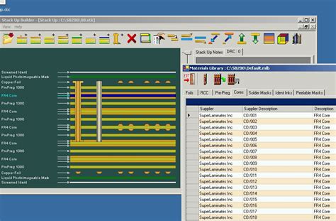
Routing and Layer Stack-up
Careful routing and layer stack-up design can significantly impact the performance of PCB transmission lines. Some key considerations include:
- Maintaining consistent trace geometry and avoiding sharp bends or discontinuities.
- Minimizing the distance between signal traces and their respective ground planes.
- Using dedicated signal layers and ground planes to minimize crosstalk and EMI.
- Avoiding routing high-speed signals near power planes or other potential noise sources.
Proper routing and layer stack-up design help to ensure signal integrity and minimize interference.

Simulation and Analysis of PCB Transmission Lines
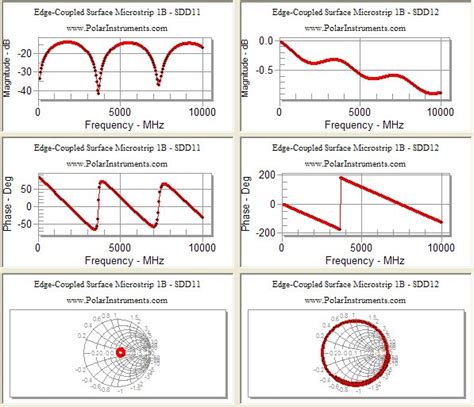
To optimize the design of PCB transmission lines, simulation and analysis tools are commonly used. These tools allow engineers to model and simulate the behavior of transmission lines under various conditions, helping to identify potential issues and optimize performance.
Electromagnetic Simulation
Electromagnetic simulation tools, such as Ansys HFSS or CST Studio Suite, enable the 3D modeling and analysis of PCB transmission lines. These tools solve Maxwell’s equations to accurately predict the electromagnetic behavior of the transmission lines, including impedance, propagation delay, and crosstalk.
Circuit Simulation
Circuit simulation tools, such as Cadence Sigrity or Keysight ADS, allow engineers to simulate the electrical behavior of PCB transmission lines in the context of the overall circuit. These tools enable the analysis of signal integrity, Power Integrity, and electromagnetic compatibility (EMC) issues.
Time-Domain Reflectometry (TDR)
Time-Domain Reflectometry (TDR) is a measurement technique used to characterize the impedance and reflections of PCB transmission lines. TDR sends a fast-rising pulse through the transmission line and measures the reflections caused by impedance discontinuities. This technique helps to identify and locate impedance mismatches, allowing for targeted design optimizations.

FAQs
-
What is the difference between microstrip and stripline transmission lines?
Microstrip transmission lines have a conductive trace on the top layer of the PCB, with a ground plane on the bottom layer. Stripline transmission lines, on the other hand, are embedded within the PCB, sandwiched between two ground planes. Stripline transmission lines offer better shielding and reduced electromagnetic interference compared to microstrip lines. -
How does the characteristic impedance of a transmission line affect signal integrity?
The characteristic impedance of a transmission line determines how well the signal is matched to the source and load impedances. If there is an impedance mismatch, reflections can occur, leading to signal distortion and degradation. Maintaining a consistent characteristic impedance throughout the transmission line is crucial for minimizing reflections and ensuring proper signal propagation. -
What are the common impedance values for PCB transmission lines?
Common impedance values for PCB transmission lines include 50Ω, 75Ω, and 100Ω. The choice of impedance depends on the specific application, the frequency of the signals, and the compatibility with other components in the system. -
What is the purpose of termination techniques in PCB transmission line design?
Termination techniques are used to minimize reflections and ensure proper signal termination at the end of the transmission line. By matching the impedance of the transmission line with the load or source impedance, termination techniques help to maintain signal integrity and prevent unwanted reflections. -
How can simulation tools help in optimizing PCB transmission line design?
Simulation tools, such as electromagnetic and circuit simulation software, allow engineers to model and analyze the behavior of PCB transmission lines under various conditions. These tools help to identify potential issues, such as impedance mismatches, crosstalk, and signal integrity problems, enabling targeted design optimizations before physical prototyping.
Conclusion
PCB transmission lines play a crucial role in ensuring the integrity and performance of high-speed and high-frequency electronic systems. By understanding the principles, characteristics, and design considerations of PCB transmission lines, engineers can effectively optimize signal integrity, minimize electromagnetic interference, and achieve robust system performance.
Proper design practices, such as impedance matching, trace geometry optimization, effective grounding and shielding, and appropriate termination techniques, are essential for the successful implementation of PCB transmission lines. Simulation and analysis tools further enhance the design process by allowing engineers to model and optimize transmission line behavior before physical prototyping.
As the demand for higher speeds and frequencies continues to grow, mastering the principles of PCB transmission lines becomes increasingly important for electronic designers. By applying the concepts and techniques discussed in this article, engineers can design reliable, high-performance PCBs that meet the ever-evolving requirements of modern electronic systems.

No responses yet