Understanding Transmission Lines
What are Transmission Lines?
Transmission lines are structures that guide electromagnetic waves from one point to another with minimal loss and distortion. In the context of PCBs, transmission lines are traces or copper paths that carry high-speed signals between components. When the signal frequencies are high enough, the traces behave like transmission lines rather than simple connections.
Why are Transmission Lines Important?
At high frequencies, the behavior of signals on PCB traces deviates from ideal conditions. The traces exhibit distributed capacitance, inductance, and resistance, leading to effects such as signal reflections, crosstalk, and impedance mismatches. These issues can severely impact signal integrity, causing problems like ringing, overshoot, undershoot, and increased electromagnetic interference (EMI).
Properly designed transmission lines help mitigate these issues by maintaining a consistent characteristic impedance along the length of the trace. This minimizes reflections and ensures clean signal propagation, reducing the risk of signal integrity problems and EMI.
Types of Transmission Lines
There are several types of transmission lines commonly used in PCB design:
Microstrip
Microstrip is the most common type of transmission line in PCBs. It consists of a trace on the top layer of the board, with a reference plane (usually ground) on the layer beneath it. The characteristic impedance of a microstrip line is determined by the trace width, thickness, and the dielectric constant of the substrate.
| Parameter | Description |
|---|---|
| W | Trace width |
| T | Trace thickness |
| H | Substrate thickness |
| Er | Relative dielectric constant of the substrate |
Stripline
Stripline is a transmission line that is sandwiched between two reference planes, typically ground planes. It offers better shielding and lower crosstalk compared to microstrip, but requires more board layers. The characteristic impedance of a stripline depends on the trace width, thickness, the distance between the reference planes, and the dielectric constant of the substrate.
| Parameter | Description |
|---|---|
| W | Trace width |
| T | Trace thickness |
| H | Distance between reference planes |
| Er | Relative dielectric constant of the substrate |
Coplanar Waveguide (CPW)
Coplanar waveguide consists of a trace with ground planes on either side, all on the same layer. CPW offers lower dispersion and better high-frequency performance compared to microstrip and stripline. The characteristic impedance of CPW depends on the trace width, the gap between the trace and ground planes, and the dielectric constant of the substrate.
| Parameter | Description |
|---|---|
| W | Trace width |
| G | Gap between trace and ground planes |
| H | Substrate thickness |
| Er | Relative dielectric constant of the substrate |
Designing Transmission Lines
Characteristic Impedance
One of the most critical aspects of transmission line design is achieving the desired characteristic impedance. The characteristic impedance (Z0) is the ratio of the voltage to the current on the line when there are no reflections. It is determined by the geometry of the trace and the properties of the substrate.
The most common characteristic impedance values used in PCB design are 50 ohms and 100 ohms. 50 ohms is widely used in RF and high-speed digital systems, while 100 ohms is often used in differential signaling schemes like LVDS and USB.
To calculate the characteristic impedance, you can use the following formulas:
Microstrip
Z0 = (87 / sqrt(Er + 1.41)) * ln(5.98 * H / (0.8 * W + T))
Stripline
Z0 = (60 / sqrt(Er)) * ln(4 * H / (0.67 * (0.8 * W + T)))
Coplanar Waveguide
Z0 = (30 * pi / sqrt(Er)) * (K(k) / K'(k))
where:
k = W / (W + 2 * G)
K(k) = pi / (ln(2 * (1 + sqrt(k')) / (1 - sqrt(k'))))
k' = sqrt(1 - k^2)
K'(k) = K(sqrt(1 - k^2))
Length Matching
In high-speed digital systems, it is often necessary to match the lengths of transmission lines to ensure synchronous arrival of signals at the receiver. Length matching helps prevent timing skew and reduces the risk of data corruption.
To calculate the length of a transmission line based on the desired delay, you can use the following formula:
Length = Delay * Velocity
where:
Velocity = c / sqrt(Er)
c = Speed of light in vacuum (approximately 3 x 10^8 m/s)
Terminations
Proper termination of transmission lines is essential to minimize reflections and ensure clean signal propagation. There are several termination schemes commonly used in PCB design:
- Series termination: A resistor is placed in series with the driver, matching the characteristic impedance of the line.
- Parallel termination: A resistor is placed at the end of the line, connecting it to a reference voltage (usually VCC or ground).
- Thevenin termination: A combination of two resistors, one connected to VCC and the other to ground, provides a parallel termination with a specific DC bias.
- AC termination: A capacitor is placed in series with the termination resistor to provide high-frequency termination while blocking DC current.
The choice of termination scheme depends on factors such as the driver characteristics, the line impedance, and the desired signal levels at the receiver.

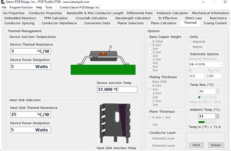
PCB Transmission Line Calculator
A PCB transmission line calculator is a software tool that simplifies the design and analysis of transmission lines on PCBs. It allows engineers to input the desired parameters and obtain the necessary trace dimensions and characteristics.
Features of a PCB Transmission Line Calculator
A comprehensive PCB transmission line calculator should offer the following features:
- Support for multiple Transmission Line Types: microstrip, stripline, and coplanar waveguide.
- Calculation of characteristic impedance based on trace geometry and substrate properties.
- Determination of trace dimensions (width and thickness) to achieve a target characteristic impedance.
- Calculation of propagation delay and phase velocity.
- Estimation of losses (conductor, dielectric, and radiation losses) based on frequency and material properties.
- Graphical representation of impedance and loss profiles over a range of frequencies.
- Ability to account for the effects of surface roughness and Skin Effect.
- Support for various substrate materials and their properties (dielectric constant, loss tangent, etc.).
- Integration with PCB design software for seamless import/export of trace parameters.
Using a PCB Transmission Line Calculator
To use a PCB transmission line calculator effectively, follow these steps:
- Select the type of transmission line (microstrip, stripline, or coplanar waveguide) based on your design requirements.
- Input the desired characteristic impedance (e.g., 50 ohms or 100 ohms) and the target frequency range.
- Specify the substrate material and its properties (dielectric constant, thickness, etc.).
- Enter any constraints on trace width, thickness, or spacing based on manufacturing capabilities or design rules.
- Run the calculator to obtain the optimal trace dimensions and characteristics.
- Analyze the results, including impedance profile, propagation delay, and losses, to ensure they meet your design goals.
- Iterate the process if necessary, adjusting parameters to optimize the transmission line performance.
- Export the calculated trace parameters to your PCB design software for implementation.
By using a PCB transmission line calculator, you can quickly and accurately design transmission lines that maintain signal integrity, minimize reflections, and ensure reliable high-speed performance.
Frequently Asked Questions (FAQ)
Q1: What is the difference between a transmission line and a regular PCB trace?
A1: A regular PCB trace is a simple connection between components, while a transmission line is a controlled-impedance structure that guides electromagnetic waves with minimal loss and distortion. Transmission lines become necessary when dealing with high-frequency signals, where the trace’s distributed capacitance, inductance, and resistance significantly impact signal behavior.
Q2: Why is characteristic impedance important in transmission line design?
A2: Characteristic impedance is a critical parameter in transmission line design because it determines how signals propagate along the line. Matching the characteristic impedance of the transmission line to the source and load impedances minimizes reflections and ensures clean signal propagation. Mismatched impedances can lead to signal integrity issues, such as ringing, overshoot, and undershoot.
Q3: How do I choose the right type of transmission line for my design?
A3: The choice of transmission line type depends on several factors, including the available board layers, the required shielding, and the target frequency range. Microstrip is the most common choice for simple designs, while stripline offers better shielding and isolation. Coplanar waveguide is useful for high-frequency applications and designs with limited board layers.
Q4: What is the purpose of length matching in transmission line design?
A4: Length matching ensures that signals traveling along different transmission lines arrive at the receiver simultaneously. This is critical in high-speed digital systems, where timing skew between signals can lead to data corruption. By matching the lengths of transmission lines, designers can minimize skew and ensure proper signal synchronization.
Q5: How does a PCB transmission line calculator help in the design process?
A5: A PCB transmission line calculator is a valuable tool that simplifies the design and analysis of transmission lines. It allows engineers to input desired parameters, such as characteristic impedance and frequency range, and obtain the necessary trace dimensions and characteristics. The calculator helps optimize the transmission line performance, reducing the risk of signal integrity issues and enabling faster design iterations.
Conclusion
Designing high-speed circuits on PCBs requires careful consideration of transmission line effects. By understanding the fundamental concepts, selecting the appropriate transmission line type, and utilizing a powerful PCB transmission line calculator, engineers can optimize signal integrity, minimize reflections, and ensure reliable performance. This comprehensive guide has provided insights into the world of PCB transmission lines, empowering you to tackle high-speed design challenges with confidence. Remember to always consider the specific requirements of your application, follow best design practices, and leverage the tools available to streamline your design process. With the right knowledge and tools, you can create robust and efficient high-speed circuits that push the boundaries of performance in the ever-evolving landscape of electronics design.
No responses yet