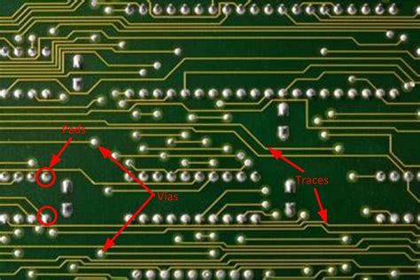
Introduction to PCB Trace Current
When designing a printed circuit board (PCB) for high voltage applications, it is crucial to consider the relationship between PCB trace width and the maximum current carrying capacity. Proper sizing of PCB traces ensures reliable operation, prevents overheating, and minimizes the risk of damage to the board and components. In this article, we will explore the factors that influence PCB trace current capacity, provide a comprehensive PCB trace width vs current table, and discuss design considerations for high voltage PCBs.
Factors Affecting PCB Trace Current Capacity
Several factors influence the current carrying capacity of a PCB trace:
1. Trace Width
The width of a PCB trace directly impacts its current carrying capacity. Wider traces have lower resistance and can handle higher currents without excessive heating. Increasing the trace width is one of the most effective ways to increase current capacity.
2. Trace Thickness
PCB trace thickness, also known as copper weight or copper thickness, affects the trace’s cross-sectional area. Thicker traces have a larger cross-sectional area, allowing them to carry more current. Standard copper weights include 0.5 oz, 1 oz, 2 oz, and 3 oz per square foot.
3. Temperature Rise
As current flows through a PCB trace, it generates heat due to the trace’s resistance. The temperature rise of the trace depends on the current, trace geometry, and the PCB’s thermal properties. Excessive temperature rise can lead to trace damage, solder joint failure, and reduced reliability.
4. Ambient Temperature
The ambient temperature surrounding the PCB also affects the trace’s current carrying capacity. Higher ambient temperatures reduce the trace’s ability to dissipate heat, limiting its current capacity. Designers must consider the maximum expected ambient temperature when determining trace sizes.
5. Trace Length
The length of a PCB trace influences its resistance and voltage drop. Longer traces have higher resistance, resulting in a greater voltage drop and increased heat generation. Designers should minimize trace lengths where possible to reduce resistance and improve current capacity.
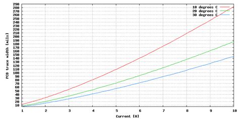
PCB Trace Width vs Current Table
The following table provides a general guideline for selecting PCB trace widths based on the desired current carrying capacity. The values assume a temperature rise of 10°C above ambient, 1 oz copper thickness (35 μm), and a trace length of 10 cm.
| Trace Width (mm) | Current Capacity (A) |
|---|---|
| 0.25 | 0.5 |
| 0.50 | 1.0 |
| 0.75 | 1.5 |
| 1.00 | 2.0 |
| 1.50 | 3.0 |
| 2.00 | 4.0 |
| 2.50 | 5.0 |
| 3.00 | 6.0 |
| 3.50 | 7.0 |
| 4.00 | 8.0 |
It is important to note that these values are approximate and may vary depending on the specific design requirements, PCB material, and environmental conditions. Designers should always refer to the manufacturer’s specifications and conduct thorough testing to ensure the PCB’s reliability and performance.

High Voltage PCB Design Considerations
When designing PCBs for high voltage applications, several additional factors must be considered to ensure safe and reliable operation:
1. Clearance and Creepage Distance
High voltage PCBs require increased clearance and creepage distances between conductors to prevent arcing and maintain electrical isolation. Clearance refers to the shortest distance through air between two conductors, while creepage is the shortest distance along the surface of the insulating material. The required clearance and creepage distances depend on the voltage level, pollution degree, and material properties.
2. Insulation Material
The choice of insulation material is critical in high voltage PCB design. Materials with high dielectric strength, such as FR-4, Rogers, and polyimide, are commonly used. The insulation material must withstand the expected voltage levels and provide adequate electrical isolation between conductors.
3. Solder Mask and Conformal Coating
Applying a solder mask and conformal coating to the PCB can enhance its high voltage performance. Solder mask helps maintain the required creepage distances and prevents solder bridging. Conformal coating provides an additional layer of insulation and protection against moisture, dust, and other environmental factors.
4. Component Selection
When selecting components for high voltage PCBs, designers must consider the voltage ratings, power dissipation, and package type. Components should have appropriate voltage and power ratings to withstand the expected operating conditions. Surface mount devices (SMDs) are often preferred over through-hole components due to their smaller size and better high-frequency performance.
5. Layout and Routing
Proper layout and routing techniques are essential for high voltage PCB design. Designers should provide adequate spacing between high voltage traces and sensitive components, avoid sharp corners and acute angles, and use ground planes to minimize electromagnetic interference (EMI) and improve signal integrity.
Frequently Asked Questions (FAQ)
1. What is the relationship between PCB trace width and current capacity?
The current carrying capacity of a PCB trace increases with its width. Wider traces have lower resistance and can handle higher currents without excessive heating. Doubling the trace width approximately doubles the current capacity, assuming other factors remain constant.
2. How does copper thickness affect PCB trace current capacity?
Copper thickness, or copper weight, influences the cross-sectional area of a PCB trace. Thicker traces have a larger cross-sectional area, allowing them to carry more current. Doubling the copper thickness while maintaining the same trace width doubles the current capacity.
3. What is the impact of temperature rise on PCB trace current capacity?
Temperature rise is a critical factor in determining PCB trace current capacity. As current flows through a trace, it generates heat due to the trace’s resistance. Excessive temperature rise can lead to trace damage, solder joint failure, and reduced reliability. Designers must consider the maximum allowable temperature rise when sizing PCB traces.
4. How do clearance and creepage distances affect high voltage PCB design?
Clearance and creepage distances are crucial in high voltage PCB design to prevent arcing and maintain electrical isolation. Clearance refers to the shortest distance through air between two conductors, while creepage is the shortest distance along the surface of the insulating material. The required clearance and creepage distances depend on the voltage level, pollution degree, and material properties. Designers must adhere to the appropriate standards and guidelines when determining these distances.
5. What are some best practices for high voltage PCB layout and routing?
When designing high voltage PCBs, it is essential to follow best practices for layout and routing. These include providing adequate spacing between high voltage traces and sensitive components, avoiding sharp corners and acute angles, and using ground planes to minimize EMI and improve signal integrity. Designers should also consider the placement of high voltage components, ensuring proper clearance and creepage distances are maintained.
Conclusion
Understanding the relationship between PCB trace width and current capacity is essential for designing reliable and high-performing PCBs, especially in high voltage applications. By considering factors such as trace width, thickness, temperature rise, ambient temperature, and trace length, designers can select appropriate trace sizes to ensure safe and efficient operation.
When designing high voltage PCBs, additional factors such as clearance and creepage distances, insulation material, solder mask and conformal coating, component selection, and layout and routing techniques must be carefully considered. By adhering to best practices and industry standards, designers can create robust and reliable high voltage PCBs that meet the demanding requirements of various applications.
No responses yet