What is a PCB Trace Width Calculator?
A PCB trace width calculator is a tool that helps designers determine the appropriate width of the traces on a PCB based on various factors such as current, temperature rise, copper thickness, and more. These calculators use mathematical formulas and industry standards to provide accurate results, ensuring that the traces can handle the required current without overheating or causing signal integrity issues.
Why is Trace Width Important in PCB Design?
Trace width plays a crucial role in PCB design for several reasons:
-
Current Carrying Capacity: The width of a trace directly affects its ability to carry current. Wider traces can handle more current without overheating, while narrower traces have a lower current carrying capacity.
-
Resistance: The resistance of a trace is inversely proportional to its width. Narrower traces have higher resistance, which can lead to voltage drops and power dissipation.
-
Signal Integrity: Trace width also impacts signal integrity. Narrower traces have higher impedance, which can cause reflections and signal distortions, especially at high frequencies.
-
Manufacturing Constraints: PCB manufacturers have limitations on the minimum trace width they can reliably produce. Designers must consider these constraints when selecting trace widths to ensure manufacturability.

Factors Affecting Trace Width Calculation
Several factors come into play when calculating the appropriate trace width for a PCB:
-
Current: The amount of current flowing through the trace is the primary factor in determining the required trace width. Higher currents require wider traces to prevent overheating and ensure reliable operation.
-
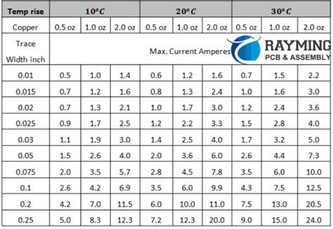
Temperature Rise: The acceptable temperature rise of the trace is another important consideration. The temperature rise depends on the ambient temperature, the maximum allowable temperature of the PCB material, and the power dissipation of the trace.
-
Copper Thickness: The thickness of the copper layer on the PCB affects the current carrying capacity of the traces. Thicker copper layers can handle more current for a given trace width.
-
Trace Length: The length of the trace also influences the required width. Longer traces have higher resistance and may require wider widths to maintain the desired current carrying capacity.
-
Voltage Drop: In some cases, the acceptable voltage drop along the trace may dictate the minimum trace width required to maintain proper circuit operation.

How to Use a PCB Trace Width Calculator
Using a PCB trace width calculator is relatively straightforward. Here’s a step-by-step guide:
-
Determine the Required Current: First, identify the maximum current that will flow through the trace. This information can be obtained from the circuit design or the component datasheets.
-
Select the Copper Thickness: Choose the appropriate copper thickness for your PCB. Common options include 0.5 oz, 1 oz, and 2 oz copper.
-
Set the Temperature Rise: Decide on the maximum acceptable temperature rise for the trace. A common value is 10°C above ambient temperature, but this can vary depending on the application and PCB material.
-
Enter the Trace Length (Optional): Some calculators allow you to input the trace length to account for its effect on resistance and voltage drop.
-
Choose the Trace Thickness (Optional): If your calculator supports different trace thicknesses, select the appropriate option. The default is usually 1.4 mils (0.0355 mm) for 1 oz copper.
-
Calculate the Trace Width: With all the required inputs provided, the calculator will determine the minimum trace width needed to meet the specified criteria. The result is typically displayed in mils or millimeters.
Here’s an example of how to use a PCB trace width calculator:
Let’s say you have a trace that needs to carry 1A of current, and you’re using 1 oz copper with a maximum acceptable temperature rise of 10°C. The trace length is 50 mm. Plugging these values into a PCB trace width calculator might yield a result like this:
| Current (A) | Copper Thickness (oz) | Temperature Rise (°C) | Trace Length (mm) | Trace Width (mm) |
|---|---|---|---|---|
| 1 | 1 | 10 | 50 | 0.4064 |
In this case, the calculator recommends a minimum trace width of 0.4064 mm (about 16 mils) to meet the specified requirements.

PCB Trace Width Calculator Tools
There are several PCB trace width calculator tools available online, both free and paid. Some popular options include:
-
Saturn PCB Toolkit: A comprehensive set of PCB design tools, including a trace width calculator.
-
EEWeb PCB Trace Width Calculator: A simple and free online calculator for determining trace widths.
-
Digi-Key PCB Trace Width Calculator: Another free online calculator with a user-friendly interface.
-
Altium PCB Toolkit: A comprehensive PCB design software package that includes a trace width calculator among other tools.
When selecting a PCB trace width calculator, consider factors such as ease of use, accuracy, and the range of input parameters supported.
Designing with Trace Width in Mind
When designing a PCB, it’s important to keep trace width considerations in mind from the start. Here are some tips for designing with trace width in mind:
-
Know Your Current Requirements: Before starting your design, make sure you have a clear understanding of the current requirements for each trace. This will help you select appropriate trace widths from the beginning.
-
Consider Voltage Drop: In addition to current, keep an eye on voltage drop, especially for longer traces or traces carrying low-voltage signals. Wider traces may be necessary to minimize voltage drop.
-
Use a PCB Layout Tool with Built-In Calculators: Many PCB layout software packages include built-in trace width calculators. Using these tools can streamline your design process and ensure that your traces are properly sized.
-
Follow Manufacturer Guidelines: Always consult your PCB manufacturer’s guidelines for minimum trace widths and spacings. Designing within these constraints will ensure that your board can be reliably manufactured.
-
Leave Some Margin: When in doubt, it’s better to err on the side of caution and use slightly wider traces than the minimum required. This provides some margin for manufacturing variability and can help improve reliability.
By following these tips and using a PCB trace width calculator, you can design PCBs with properly sized traces that meet your current, temperature, and signal integrity requirements.
Frequently Asked Questions (FAQ)
-
Q: What happens if I use traces that are too narrow for my current requirements?
A: Using traces that are too narrow can lead to several problems, including overheating, excessive voltage drop, and reduced reliability. In extreme cases, overly narrow traces can even cause the PCB to fail. -
Q: Can I use the same trace width for all the traces on my PCB?
A: Not necessarily. Each trace should be sized according to its specific current, temperature, and voltage drop requirements. Some traces may need to be wider than others depending on their function and location on the board. -
Q: How do I account for temperature rise when calculating trace widths?
A: Most PCB trace width calculators include a field for specifying the maximum acceptable temperature rise. This value is typically set to 10°C above ambient, but can be adjusted based on your specific requirements and the PCB material’s thermal properties. -
Q: What is the difference between internal and external traces when it comes to trace width?
A: Internal traces (those on inner layers of the PCB) can usually be narrower than external traces (those on the top or bottom layers) for a given current requirement. This is because internal traces are surrounded by PCB material, which helps dissipate heat more effectively. -
Q: Can I use a PCB trace width calculator for high-frequency signals?
A: While a trace width calculator can provide a starting point for high-frequency signal traces, other factors such as impedance control and signal integrity also come into play. For high-speed designs, it’s best to use specialized tools and follow design guidelines specific to high-frequency PCBs.
By understanding the role of trace width in PCB design and using a PCB trace width calculator, you can create designs that are reliable, manufacturable, and meet your performance requirements. Always double-check your calculations and consult with your PCB manufacturer to ensure the best possible results.
No responses yet