Introduction to PCB Capacitance
Printed Circuit Board (PCB) design involves many crucial aspects, one of which is managing the capacitance between traces and planes. Understanding the concept of PCB capacitance and how to calculate it using the appropriate formula is essential for designing high-quality, reliable electronic circuits. In this article, we will delve into the world of PCB trace to plane capacitance, explore the factors that influence it, and provide a comprehensive guide on how to calculate it using the PCB capacitance formula.
What is PCB Capacitance?
PCB capacitance refers to the electrical property of a printed circuit board that allows it to store electrical charge between its conductive surfaces, such as traces and planes. This capacitance is an inherent characteristic of the PCB and can have both positive and negative effects on the performance of the electronic circuit.
Why is PCB Capacitance Important?
Managing PCB capacitance is crucial for several reasons:
-
Signal Integrity: Excessive capacitance can lead to signal distortion, crosstalk, and slower signal propagation, which can negatively impact the overall performance of the circuit.
-
Electromagnetic Compatibility (EMC): Proper management of PCB capacitance helps in reducing electromagnetic interference (EMI) and ensuring compliance with EMC regulations.
-
Power Integrity: Capacitance between power planes and ground planes can help reduce Power Supply Noise and maintain stable voltage levels.
-
Impedance Matching: Controlling the capacitance between traces and planes is essential for achieving proper impedance matching, which is critical for high-speed digital circuits.
Factors Affecting PCB Trace to Plane Capacitance
Several factors influence the capacitance between a PCB trace and a plane. Understanding these factors is crucial for accurately calculating and managing PCB capacitance.
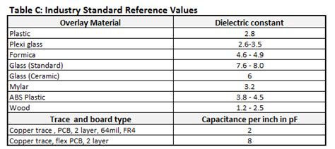
Dielectric Constant (εr)
The dielectric constant, also known as relative permittivity, is a material property that describes how easily an electric field can be established in a material compared to a vacuum. In PCBs, the dielectric constant of the substrate material significantly affects the capacitance between traces and planes. Common PCB Substrate Materials and their typical dielectric constants are:
| Material | Dielectric Constant (εr) |
|---|---|
| FR-4 | 4.2 – 4.5 |
| Rogers RO4003C | 3.38 |
| Polyimide | 3.2 – 3.5 |
| PTFE (Teflon) | 2.1 |
A higher dielectric constant leads to higher capacitance between traces and planes.
Trace Width (w)
The width of the PCB trace directly affects its capacitance to the plane. A wider trace results in higher capacitance, as it increases the surface area facing the plane. Trace width is typically determined by the current carrying requirements and the desired characteristic impedance of the trace.
Trace Thickness (t)
The thickness of the copper trace also influences its capacitance to the plane. A thicker trace has a greater surface area, resulting in higher capacitance. However, the effect of trace thickness on capacitance is less significant compared to trace width.
Distance between Trace and Plane (h)
The distance between the PCB trace and the plane, often determined by the thickness of the dielectric substrate, is another crucial factor affecting capacitance. A smaller distance between the trace and plane leads to higher capacitance, as the electric field strength increases with decreasing distance.
PCB Trace to Plane Capacitance Formula
The capacitance between a PCB trace and a plane can be calculated using the following formula:
C = (εr × ε0 × A) / h
Where:
– C is the capacitance in farads (F)
– εr is the dielectric constant of the substrate material
– ε0 is the permittivity of free space (8.85 × 10^-12 F/m)
– A is the area of the trace facing the plane in square meters (m^2)
– h is the distance between the trace and the plane in meters (m)
To calculate the area (A) of the trace facing the plane, use the following formula:
A = w × l
Where:
– w is the width of the trace in meters (m)
– l is the length of the trace in meters (m)
It’s important to note that this formula assumes a parallel plate capacitor model and does not take into account fringing effects or the presence of nearby traces or planes. For more accurate capacitance calculations, advanced tools such as electromagnetic field solvers or specialized PCB Design software can be used.
Example Calculation
Let’s calculate the capacitance between a PCB trace and a plane using the following parameters:
- Dielectric constant (εr) of FR-4 substrate: 4.3
- Trace width (w): 0.2 mm (0.0002 m)
- Trace length (l): 50 mm (0.05 m)
- Distance between trace and plane (h): 0.1 mm (0.0001 m)
Step 1: Calculate the area (A) of the trace facing the plane
A = w × l
A = 0.0002 m × 0.05 m
A = 1 × 10^-5 m^2
Step 2: Apply the PCB trace to plane capacitance formula
C = (εr × ε0 × A) / h
C = (4.3 × 8.85 × 10^-12 F/m × 1 × 10^-5 m^2) / 0.0001 m
C = 3.8055 × 10^-13 F
C ≈ 0.38 pF
In this example, the capacitance between the PCB trace and the plane is approximately 0.38 picofarads (pF).

Managing PCB Trace to Plane Capacitance
Now that we understand the factors affecting PCB trace to plane capacitance and how to calculate it using the formula, let’s explore some strategies for managing capacitance in PCB design.
Choosing the Right Substrate Material
Selecting an appropriate substrate material with a suitable dielectric constant is crucial for managing PCB capacitance. For high-speed digital circuits or applications requiring low capacitance, consider using substrates with lower dielectric constants, such as PTFE (Teflon) or Rogers RO4003C. However, keep in mind that these materials may have higher costs and more complex manufacturing requirements compared to standard FR-4.
Adjusting Trace Geometry
Modifying the width and thickness of PCB traces can help in managing capacitance. Narrower traces result in lower capacitance, but they may also have higher current densities and increased resistance. Striking a balance between trace width and capacitance requirements is essential for optimal circuit performance.
Increasing the Distance between Trace and Plane
Increasing the distance between the PCB trace and the plane, either by using thicker substrates or by placing the trace on a different layer, can effectively reduce capacitance. However, this approach may impact the overall thickness of the PCB and increase manufacturing costs.
Using Ground Planes and Power Planes
Incorporating dedicated ground planes and power planes in the PCB design helps in managing capacitance and improving signal integrity. These planes provide a low-impedance return path for signals and help in reducing crosstalk and electromagnetic interference. By carefully placing traces in relation to these planes, designers can optimize capacitance and maintain signal integrity.
Employing Shielding Techniques
In some cases, shielding techniques can be used to manage PCB capacitance and reduce crosstalk between traces. Shielding involves placing grounded traces or planes adjacent to sensitive signal traces, effectively creating a barrier that minimizes electromagnetic interaction. This technique is particularly useful in high-speed digital circuits or applications with strict EMC requirements.
Frequently Asked Questions (FAQ)
-
Q: What is the difference between capacitance and inductance in PCBs?
A: Capacitance is the ability of a PCB to store electrical charge between conductive surfaces, while inductance is the property of a conductor to resist changes in current flow. Both capacitance and inductance can affect signal integrity and must be carefully managed in PCB design. -
Q: How does the dielectric constant of a substrate material affect PCB capacitance?
A: The dielectric constant of a substrate material directly influences the capacitance between PCB traces and planes. A higher dielectric constant leads to higher capacitance, as it allows for easier establishment of electric fields within the material. -
Q: Can PCB capacitance be used intentionally in circuit design?
A: Yes, PCB capacitance can be intentionally used in certain circuit designs. For example, power plane to ground plane capacitance can help in reducing power supply noise and providing local decoupling. However, in most cases, PCB capacitance is an unintended consequence that needs to be managed and minimized. -
Q: What are some common issues caused by excessive PCB capacitance?
A: Excessive PCB capacitance can lead to various issues, such as signal distortion, crosstalk, slower signal propagation, and increased electromagnetic interference (EMI). These issues can negatively impact the performance and reliability of the electronic circuit. -
Q: Are there any software tools available for calculating PCB capacitance?
A: Yes, there are several software tools available that can help in calculating PCB capacitance. These tools include electromagnetic field solvers, such as Ansys HFSS or CST Studio Suite, and specialized PCB design software with built-in capacitance calculators, such as Altium Designer or Cadence Allegro. These tools provide more accurate results by considering factors like fringing effects and the presence of nearby traces or planes.
Conclusion
Understanding and managing PCB trace to plane capacitance is crucial for designing high-quality, reliable electronic circuits. By considering factors such as the dielectric constant of the substrate material, trace geometry, and the distance between the trace and plane, designers can effectively calculate and optimize capacitance using the PCB capacitance formula.
Employing strategies like selecting appropriate substrate materials, adjusting trace geometry, increasing the distance between traces and planes, using dedicated ground and power planes, and implementing shielding techniques can help in managing PCB capacitance and ensuring optimal circuit performance.
As PCB design becomes increasingly complex, with higher signal speeds and stricter EMC requirements, the importance of understanding and managing PCB capacitance cannot be overstated. By mastering the concepts and techniques discussed in this article, PCB designers can create robust, reliable, and high-performance electronic circuits that meet the demands of modern applications.
No responses yet