What is PCB Trace Thickness?
PCB trace thickness refers to the thickness of the copper traces that carry electrical signals and power between components on a printed circuit board. The thickness of these traces is typically measured in ounces of copper per square foot (oz/ft²) or in microns (µm).
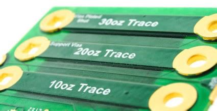
The most common PCB trace thicknesses are:
| Thickness (oz/ft²) | Thickness (µm) |
|---|---|
| 0.5 oz/ft² | 17.5 µm |
| 1 oz/ft² | 35 µm |
| 2 oz/ft² | 70 µm |
| 3 oz/ft² | 105 µm |
| 4 oz/ft² | 140 µm |
Factors Influencing PCB Trace Thickness Selection
When selecting the appropriate PCB trace thickness for your design, several factors must be considered:
Current Carrying Capacity
The current carrying capacity of a PCB trace is directly related to its cross-sectional area, which is determined by its width and thickness. Thicker traces can carry more current without overheating, making them suitable for power-hungry applications or high-current signals.
Voltage Drop
Voltage drop occurs when current flows through a trace, causing a decrease in voltage along the length of the trace. Thicker traces have lower resistance, resulting in reduced voltage drop and improved signal integrity.
High-Speed Signals
For high-speed signals, such as those found in high-frequency digital circuits, the trace thickness can impact the characteristic impedance of the trace. Maintaining a consistent characteristic impedance is essential for minimizing signal reflections and ensuring proper signal propagation.
Manufacturing Constraints
The choice of PCB trace thickness is also influenced by manufacturing constraints. Thinner traces are more challenging to manufacture and have tighter tolerances, which can increase production costs. Thicker traces, on the other hand, may require more etching time and consume more copper, affecting the overall cost and production time.

PCB Trace Thickness Guidelines
To ensure optimal performance and manufacturability, follow these guidelines when selecting PCB trace thicknesses:
Power Traces
For power traces, use thicker copper to minimize voltage drop and handle higher currents. A good rule of thumb is to use 1 oz/ft² copper for every 1 A of current.
Signal Traces
For signal traces, the thickness should be selected based on the signal speed and required characteristic impedance. Consult with your PCB manufacturer or use impedance calculators to determine the appropriate thickness for your design.
Thermal Management
In applications where thermal management is critical, using thicker copper traces can help dissipate heat more effectively. This is particularly important for power-intensive components or high-current traces.
Manufacturing Tolerances
Always consider the manufacturing tolerances when selecting PCB trace thicknesses. Consult with your PCB manufacturer to understand their capabilities and limitations, and design your traces accordingly.

PCB Trace Thickness Calculation
To calculate the appropriate PCB trace thickness for your design, you can use various online tools and calculators. These tools take into account factors such as current carrying capacity, trace width, temperature rise, and more.
Some popular PCB trace thickness calculators include:
By inputting your design requirements into these calculators, you can quickly determine the appropriate PCB trace thickness for your specific application.

Advanced Topics in PCB Trace Thickness
High-Current Applications
In high-current applications, such as power electronics or automotive systems, using thicker copper traces may not be sufficient to handle the required current. In these cases, additional techniques can be employed, such as:
- Using multiple parallel traces to distribute the current
- Implementing copper pours or planes to increase the cross-sectional area
- Using thicker PCBs with multiple copper layers
High-Frequency Applications
For high-frequency applications, the skin effect and dielectric losses become significant factors in determining the appropriate PCB trace thickness. The skin effect causes high-frequency currents to flow primarily on the surface of the conductor, effectively reducing the cross-sectional area of the trace.
To mitigate the skin effect and dielectric losses, consider the following:
- Use thinner traces to minimize the skin effect
- Choose low-loss dielectric materials to reduce dielectric losses
- Implement controlled impedance traces to maintain signal integrity
Flex PCBs
Flexible PCBs have unique requirements when it comes to trace thickness. Thinner traces are often preferred to maintain flexibility and reduce stress on the copper during bending. However, this must be balanced with the current carrying capacity and signal integrity requirements of the design.
When designing flex PCBs, consider the following:
- Use thinner copper traces (e.g., 0.5 oz/ft² or 1 oz/ft²) to maintain flexibility
- Implement strain relief features, such as curved traces or accordion-style bends
- Use additional support layers, such as polyimide or adhesives, to reinforce the traces
Frequently Asked Questions (FAQ)
-
What is the most common PCB trace thickness?
The most common PCB trace thickness is 1 oz/ft² (35 µm). This thickness provides a good balance between current carrying capacity, signal integrity, and manufacturability for most applications. -
Can I mix different trace thicknesses on the same PCB?
Yes, it is possible to use different trace thicknesses on the same PCB. This is often done to optimize current carrying capacity, signal integrity, and thermal management for different parts of the circuit. However, keep in mind that using multiple trace thicknesses can increase manufacturing complexity and cost. -
How does PCB trace thickness affect impedance?
PCB trace thickness, along with trace width and dielectric properties, determines the characteristic impedance of a trace. Thicker traces generally have lower impedance, while thinner traces have higher impedance. To maintain a specific characteristic impedance, the trace width must be adjusted in conjunction with the thickness. -
What happens if I use traces that are too thin for my application?
Using traces that are too thin for your application can lead to several issues, such as: - Insufficient current carrying capacity, leading to overheating and potential trace damage
- Increased voltage drop, affecting signal integrity and power delivery
-
Reduced mechanical strength, making the traces more susceptible to damage during handling or operation
-
How can I determine the appropriate trace thickness for my PCB design?
To determine the appropriate trace thickness for your PCB design, follow these steps: - Identify the current carrying requirements for power traces and use the rule of thumb (1 oz/ft² per 1 A) as a starting point
- Consider the signal speed and required characteristic impedance for signal traces, and use impedance calculators or consult with your PCB manufacturer
- Evaluate thermal management needs and use thicker traces for power-intensive components or high-current traces
- Review manufacturing tolerances and capabilities with your PCB manufacturer and adjust your design accordingly
Conclusion
PCB trace thickness is a critical aspect of printed circuit board design that directly impacts the performance, reliability, and manufacturability of the final product. By understanding the factors that influence trace thickness selection, following design guidelines, and using appropriate calculation tools, you can ensure that your PCB design meets the required specifications while optimizing cost and production efficiency.
Remember to consider current carrying capacity, voltage drop, high-speed signals, thermal management, and manufacturing constraints when selecting PCB trace thicknesses. Additionally, consult with your PCB manufacturer to understand their capabilities and limitations, and design your traces accordingly.
By keeping these factors in mind and following the guidelines outlined in this article, you can create PCB designs that are robust, reliable, and manufacturable, ultimately leading to successful electronic products.
No responses yet