Introduction to PCB Traces
PCB traces are the copper pathways that electrically connect the various components on a printed circuit board (PCB). They are essential for the proper functioning of the PCB and play a critical role in the overall performance and reliability of the electronic device. In this article, we will delve into the importance of PCB traces, their design considerations, and best practices for optimizing their performance.
What are PCB Traces?
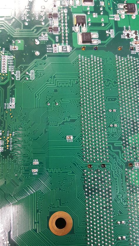
PCB traces are the conductive paths that are etched or printed onto the surface of a PCB. They are typically made of copper and are used to carry electrical signals and power between the various components on the board. The width, thickness, and spacing of the traces are carefully designed to ensure optimal signal integrity and to minimize interference and crosstalk.
The Role of PCB Traces in PCB Design
PCB traces play a crucial role in the overall design of a PCB. They are responsible for carrying the electrical signals between the various components on the board, such as integrated circuits, resistors, capacitors, and connectors. The proper design of PCB traces is essential for ensuring the reliability and performance of the electronic device.
PCB Trace Design Considerations
Trace Width and Thickness
The width and thickness of PCB traces are critical factors in their performance. The width of the trace determines its current-carrying capacity, while the thickness affects its resistance and impedance. Wider traces can carry more current, but they also take up more space on the PCB. Thicker traces have lower resistance and impedance, but they are more expensive to manufacture.
| Trace Width (mils) | Current Capacity (A) |
|---|---|
| 10 | 0.5 |
| 20 | 1.0 |
| 30 | 1.5 |
| 40 | 2.0 |
| 50 | 2.5 |
Table 1: Current Capacity vs. Trace Width
Trace Spacing and Clearance
The spacing between PCB traces is another important consideration. The minimum spacing between traces is determined by the manufacturing process and the voltage level of the signals. Higher voltage signals require greater spacing to prevent arcing and short circuits. The clearance between traces and other components on the PCB must also be carefully designed to avoid interference and signal integrity issues.
Impedance Matching
Impedance matching is the process of designing PCB traces to have a specific characteristic impedance. This is important for high-speed digital signals, where reflections and signal distortion can occur if the impedance of the trace does not match the impedance of the source and load. Impedance matching is achieved by carefully controlling the width, thickness, and spacing of the traces, as well as the dielectric constant of the PCB material.
Crosstalk and EMI
Crosstalk and electromagnetic interference (EMI) are two common issues that can affect the performance of PCB traces. Crosstalk occurs when signals on adjacent traces interfere with each other, causing signal distortion and errors. EMI occurs when external electromagnetic fields interfere with the signals on the PCB traces. Both of these issues can be minimized by careful design of the PCB layout and the use of shielding and filtering techniques.

Best Practices for PCB Trace Design
Use a Ground Plane
Using a ground plane is one of the best ways to improve the performance of PCB traces. A ground plane is a large area of copper on the PCB that is connected to the ground potential. It provides a low-impedance path for return currents and helps to minimize crosstalk and EMI. The ground plane should be placed as close to the signal traces as possible to maximize its effectiveness.
Keep Traces Short and Direct
Keeping PCB traces as short and direct as possible is another best practice for optimizing their performance. Longer traces have higher resistance and are more susceptible to noise and interference. Direct traces also minimize the amount of space required on the PCB, which can help to reduce manufacturing costs.
Avoid Sharp Bends and Corners
Sharp bends and corners in PCB traces can cause signal reflections and distortions. It is best to use smooth, gradual curves instead of sharp angles. If a sharp bend is unavoidable, it is recommended to use a mitered corner to minimize the reflections.
Use Differential Pairs for High-Speed Signals
For high-speed digital signals, it is recommended to use differential pairs instead of single-ended traces. Differential pairs consist of two traces that carry the same signal but with opposite polarity. This helps to cancel out any noise or interference that may be present on the traces. Differential pairs also have better signal integrity and are less susceptible to crosstalk and EMI.
Consider the PCB Material
The choice of PCB material can also have a significant impact on the performance of PCB traces. Different materials have different dielectric constants, which affect the impedance and propagation speed of the signals. For high-speed designs, it is recommended to use materials with low dielectric constants, such as Rogers or Isola, to minimize signal distortion and loss.

PCB Trace Routing Techniques
Manual Routing
Manual routing is the process of manually placing and routing PCB traces using PCB design software. This technique provides the greatest control over the placement and routing of the traces, but it can be time-consuming and requires a high level of skill and experience.
Autorouting
Autorouting is the process of using software algorithms to automatically place and route PCB traces. This technique is faster and less labor-intensive than manual routing, but it may not always produce the most optimal results. Autorouting algorithms can struggle with complex designs and may not always follow best practices for trace placement and routing.
Hybrid Routing
Hybrid routing is a combination of manual and autorouting techniques. This approach involves manually placing critical traces and components, and then using autorouting to fill in the remaining traces. Hybrid routing can provide a good balance between control and efficiency, and can help to ensure that critical traces are placed and routed optimally.

PCB Trace Testing and Verification
Continuity Testing
Continuity testing is the process of verifying that PCB traces are electrically connected as intended. This is typically done using a multimeter or a dedicated continuity tester. Continuity testing can help to identify any open or short circuits in the traces, which can cause the PCB to malfunction.
Impedance Testing
Impedance testing is the process of measuring the characteristic impedance of PCB traces. This is important for high-speed designs, where impedance matching is critical for signal integrity. Impedance testing can be done using a time-domain reflectometer (TDR) or a vector network analyzer (VNA).
Signal Integrity Analysis
Signal integrity analysis is the process of simulating and measuring the behavior of signals on PCB traces. This can help to identify any issues with signal reflections, crosstalk, or EMI, and can guide the design of the PCB to minimize these issues. Signal integrity analysis can be done using specialized software tools, such as HyperLynx or Sigrity.
Advanced PCB Trace Techniques
Controlled Impedance Routing
Controlled impedance routing is a technique for designing PCB traces with a specific characteristic impedance. This is achieved by carefully controlling the width, thickness, and spacing of the traces, as well as the dielectric constant of the PCB material. Controlled impedance routing is essential for high-speed designs, where impedance matching is critical for signal integrity.
High-Density Interconnect (HDI)
High-density interconnect (HDI) is a technique for designing PCBs with very small trace widths and spacings. HDI designs can pack more functionality into a smaller area, but they require advanced manufacturing processes and materials. HDI designs also require careful attention to signal integrity and power delivery, as the smaller traces are more susceptible to noise and interference.
Rigid-Flex PCBs
Rigid-flex PCBs are a type of PCB that combines rigid and flexible substrates. The flexible portions of the PCB allow the board to bend and fold, which can be useful for applications where space is limited or where the PCB needs to conform to a specific shape. Rigid-flex PCBs require special design considerations for the placement and routing of traces, as well as for the mechanical stresses on the board.
Frequently Asked Questions (FAQ)
What is the difference between a PCB trace and a wire?
A PCB trace is a conductive pathway that is etched or printed onto the surface of a PCB, while a wire is a separate conductor that is attached to the PCB. PCB traces are typically made of copper and are an integral part of the PCB, while wires are separate components that are soldered or attached to the PCB.
How do I calculate the current carrying capacity of a PCB trace?
The current carrying capacity of a PCB trace depends on its width, thickness, and the temperature rise of the board. There are various online calculators and charts available that can help to estimate the current carrying capacity of a trace based on these parameters. As a general rule of thumb, wider and thicker traces can carry more current than narrower and thinner traces.
What is the minimum spacing between PCB traces?
The minimum spacing between PCB traces depends on the manufacturing process and the voltage level of the signals. For standard PCB manufacturing processes, the minimum spacing is typically around 5-10 mils (0.005-0.010 inches). For high-voltage signals, the minimum spacing may need to be increased to prevent arcing and short circuits.
How do I prevent crosstalk between PCB traces?
Crosstalk between PCB traces can be minimized by careful design of the PCB layout. Some techniques for preventing crosstalk include:
- Keeping sensitive traces away from noisy traces
- Using ground planes to provide shielding between traces
- Using differential pairs for high-speed signals
- Adding guard traces or shielding around sensitive traces
What is the best way to route PCB traces for high-speed signals?
For high-speed signals, it is best to use controlled impedance routing techniques to ensure that the traces have a specific characteristic impedance. This involves carefully controlling the width, thickness, and spacing of the traces, as well as the dielectric constant of the PCB material. It is also recommended to use differential pairs for high-speed signals, as they have better signal integrity and are less susceptible to crosstalk and EMI.
Conclusion
PCB traces are the lifeblood of any PCB design. They are responsible for carrying electrical signals and power between the various components on the board, and their proper design is essential for ensuring the reliability and performance of the electronic device. In this article, we have explored the importance of PCB traces, their design considerations, and best practices for optimizing their performance.
We have covered topics such as trace width and thickness, spacing and clearance, impedance matching, crosstalk and EMI, and various routing techniques. We have also discussed advanced techniques such as controlled impedance routing, HDI, and rigid-flex PCBs.
By following the best practices and techniques outlined in this article, PCB designers can create robust and reliable PCBs that meet the performance requirements of their applications. Whether you are a seasoned PCB designer or just starting out, understanding the importance of PCB traces is essential for creating high-quality PCBs that stand the test of time.
No responses yet