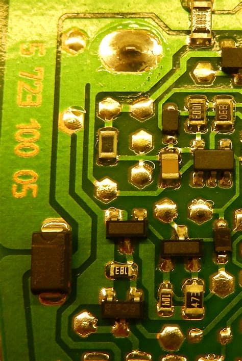
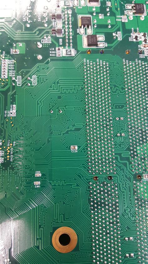
What are PCB Traces?
PCB traces are the copper pathways THAt are etched or printed onto the surface of a PCB. They connect various components, such as resistors, capacitors, and integrated circuits, allowing electrical signals to flow between them. The width, thickness, and spacing of these traces play a critical role in determining the performance and reliability of the PCB.
Types of PCB Traces
There are several types of PCB traces, each with its own characteristics and applications:
-
Signal Traces: These traces carry low-power signals between components and are the most common type of traces found on a PCB.
-
Power Traces: These traces are used to distribute power from the power source to various components on the PCB. They are typically wider and thicker than signal traces to handle higher currents.
-
Ground Traces: Ground traces are used to provide a common reference point for electrical signals and to minimize noise and interference. They are often connected to a ground plane, which is a large area of copper on the PCB.
-
High-Speed Traces: These traces are designed to carry high-frequency signals, such as those found in high-speed digital circuits. They require special design considerations to minimize signal distortion and maintain signal integrity.
PCB Trace Design Considerations
Designing PCB traces involves several key considerations to ensure optimal performance and reliability. Some of the most important factors include:
Trace Width and Thickness
The width and thickness of a PCB trace determine its electrical resistance and current-carrying capacity. Wider and thicker traces have lower resistance and can carry more current, while narrower and thinner traces have higher resistance and are better suited for low-power signals. The appropriate trace width and thickness depend on factors such as the current requirements, the PCB material, and the manufacturing process.
Trace Spacing
Trace spacing refers to the distance between adjacent traces on a PCB. Proper spacing is essential to minimize crosstalk, which is the unwanted coupling of signals between traces. The minimum trace spacing depends on factors such as the signal frequency, the PCB material, and the manufacturing process. In general, higher-frequency signals require greater trace spacing to minimize crosstalk.
Trace Length and Routing
The length and routing of PCB traces can have a significant impact on signal integrity and performance. Longer traces are more susceptible to signal degradation and noise, while shorter traces minimize these effects. When routing traces, it is important to minimize the number of vias (holes that connect traces on different layers) and to avoid sharp bends or corners, which can cause signal reflections and distortions.
Impedance Matching
Impedance matching is the process of designing PCB traces to have a specific characteristic impedance, which is determined by factors such as the trace width, thickness, and spacing, as well as the PCB material properties. Proper impedance matching is essential for high-speed digital circuits to minimize signal reflections and ensure signal integrity.
PCB Trace Materials
PCB traces are typically made of copper due to its excellent electrical conductivity and relatively low cost. However, there are several types of copper used in PCB manufacturing, each with its own properties and applications:
-
Standard Copper: This is the most common type of copper used in PCB manufacturing. It has good electrical conductivity and is suitable for most applications.
-
Low-Profile Copper: This type of copper is thinner than standard copper and is used in high-density PCB designs where space is limited.
-
High-Temp Copper: This type of copper is designed to withstand higher temperatures and is used in applications where the PCB is exposed to extreme heat, such as in automotive or aerospace electronics.
-
Rolled Annealed Copper: This type of copper is specially processed to have a finer grain structure, which improves its mechanical and electrical properties. It is often used in high-reliability applications, such as medical devices or military equipment.

PCB Trace Manufacturing Processes
There are several manufacturing processes used to create PCB traces, each with its own advantages and limitations:
-
Etching: This is the most common method for creating PCB traces. It involves applying a photoresist layer to the copper surface, exposing it to light through a patterned mask, and then chemically etching away the unwanted copper.
-
Milling: This method uses a precision milling machine to remove unwanted copper from the PCB surface, leaving behind the desired trace pattern. Milling is often used for prototyping or low-volume production.
-
Printing: This method involves printing the trace pattern directly onto the PCB surface using conductive ink or paste. Printing is a relatively new technology and is still being developed for high-volume production.
Advanced PCB Trace Techniques
In addition to the basic design considerations, there are several advanced techniques that can be used to optimize PCB trace performance and reliability:
Differential Pairs
Differential pairs are two traces that carry a differential signal, which is a pair of signals that are equal in magnitude but opposite in polarity. Differential pairs are often used in high-speed digital circuits to minimize noise and crosstalk. When designing differential pairs, it is important to maintain a constant spacing between the traces and to route them as closely together as possible.
Microstrip and Stripline
Microstrip and stripline are two common types of transmission lines used in High-Speed PCB designs. Microstrip consists of a single trace on the top layer of the PCB, with a ground plane on the bottom layer. Stripline consists of a single trace sandwiched between two ground planes. Both microstrip and stripline require careful design to maintain the desired characteristic impedance and minimize signal reflections.
Controlled impedance
Controlled impedance is a technique used to maintain a specific characteristic impedance along the length of a PCB trace. This is achieved by carefully controlling the trace width, thickness, and spacing, as well as the PCB material properties. Controlled impedance is essential for high-speed digital circuits to ensure signal integrity and minimize reflections.
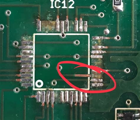
PCB Trace Testing and Inspection
Once a PCB has been manufactured, it is important to test and inspect the traces to ensure they meet the desired specifications and are free of defects. Some common testing and inspection methods include:
-
Visual Inspection: This involves visually examining the PCB traces under magnification to check for defects such as shorts, opens, or incorrect trace widths.
-
Continuity Testing: This involves using a multimeter or other test equipment to verify that each trace is electrically continuous from end to end.
-
Time-Domain Reflectometry (TDR): This is a technique used to measure the impedance and signal integrity of PCB traces. It involves sending a high-frequency pulse down the trace and analyzing the reflected signal to detect any impedance discontinuities or other anomalies.
-
X-Ray Inspection: This involves using X-ray imaging to examine the internal structure of the PCB, including the traces and vias. X-ray inspection can detect defects that are not visible on the surface, such as voids or delamination.
Frequently Asked Questions (FAQ)
-
What is the difference between a PCB trace and a wire?
A PCB trace is a flat, conductive pathway that is etched or printed onto the surface of a PCB, while a wire is a separate, insulated conductor that is used to connect components or PCBs together. PCB traces are an integral part of the PCB, while wires are external to the PCB. -
Can PCB traces be repaired if they are damaged?
Yes, PCB traces can be repaired using techniques such as jumper wires, conductive epoxy, or trace repair kits. However, the effectiveness of the repair depends on the extent of the damage and the skill of the technician. In some cases, it may be more cost-effective to replace the entire PCB. -
What is the minimum trace width and spacing that can be achieved with current PCB manufacturing technology?
The minimum trace width and spacing depend on the PCB manufacturing process and the capabilities of the manufacturer. With current technology, trace widths as small as 3 mil (0.003 inches) and spacing as small as 3 mil can be achieved. However, these dimensions may increase the cost and complexity of the PCB manufacturing process. -
How do I calculate the appropriate trace width for a given current requirement?
There are several online calculators and charts available that can help you determine the appropriate trace width for a given current requirement, based on factors such as the PCB material, copper thickness, and temperature rise. In general, wider traces are needed for higher currents, and the trace width should be selected to keep the temperature rise within acceptable limits. -
What is the difference between a single-ended trace and a differential pair?
A single-ended trace carries a signal that is referenced to a common ground, while a differential pair carries a differential signal that is referenced to itself. Differential pairs are often used in high-speed digital circuits to minimize noise and crosstalk, while single-ended traces are used for lower-speed signals or when noise is less of a concern.
Conclusion
PCB traces are the lifeblood of any electronic device, carrying electrical signals between components and enabling the device to function as intended. Designing, manufacturing, and testing PCB traces requires a deep understanding of electrical principles, materials science, and manufacturing processes. By carefully considering factors such as trace width, thickness, spacing, and routing, engineers can create PCBs that are reliable, efficient, and cost-effective. As PCB technology continues to evolve, new materials and manufacturing processes will undoubtedly emerge, enabling even greater performance and miniaturization. However, the fundamental principles of PCB trace design will remain essential for creating high-quality electronic devices that meet the needs of a wide range of applications.
No responses yet