Introduction to PCB Clearance
Printed Circuit Board (PCB) design is a crucial aspect of electronic product development. One of the most important considerations in PCB design is the clearance between traces and pads, especially when dealing with different voltage levels. Proper clearance ensures the reliability, safety, and functionality of the PCB. In this article, we will explore the differences between low and high voltage PCB trace and pad clearance requirements.
Understanding PCB Trace and Pad Clearance
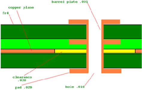
PCB trace and pad clearance refers to the minimum distance between two conductive elements on a PCB. This distance is necessary to prevent electrical shorts, arcing, and other issues that can arise due to insufficient spacing. The clearance requirements vary depending on the voltage levels involved in the circuit.
Factors Affecting PCB Clearance
Several factors influence the required PCB trace and pad clearance:
- Voltage level: Higher voltages require greater clearance distances to prevent arcing and maintain insulation.
- PCB material: The dielectric strength of the PCB material affects the required clearance. Higher dielectric strength materials allow for smaller clearances.
- Environmental conditions: Factors such as humidity, temperature, and altitude can impact the necessary clearance distances.
- Manufacturing capabilities: The minimum achievable clearance is limited by the manufacturing process and equipment used.

Low Voltage PCB Clearance
Low voltage PCBs typically operate at voltages below 50V. These circuits are commonly found in consumer electronics, such as smartphones, laptops, and IoT devices. The clearance requirements for low voltage PCBs are generally smaller compared to high voltage PCBs.
IPC Standards for Low Voltage Clearance
The IPC (Association Connecting Electronics Industries) provides guidelines for PCB design, including recommended clearance distances. For low voltage PCBs, the relevant standard is IPC-2221B. This standard defines the minimum clearance based on the peak voltage between two conductors.
| Peak Voltage (V) | Minimum Clearance (mm) |
|---|---|
| 0-15 | 0.05 |
| 16-30 | 0.1 |
| 31-50 | 0.6 |
Table 1: IPC-2221B Low Voltage Clearance Requirements
Design Considerations for Low Voltage PCBs
When designing low voltage PCBs, consider the following:
- Use appropriate trace widths to ensure sufficient current carrying capacity and minimize voltage drop.
- Maintain consistent trace spacing to avoid signal integrity issues, such as crosstalk.
- Follow the recommended clearance distances based on the peak voltage levels in the circuit.
- Consider using ground planes to improve signal integrity and reduce electromagnetic interference (EMI).

High Voltage PCB Clearance
High voltage PCBs operate at voltages above 50V and can reach several kilovolts in some applications. These circuits are found in power electronics, automotive systems, and industrial equipment. The clearance requirements for high voltage PCBs are more stringent to ensure safe operation and prevent electrical breakdown.
Standards for High Voltage Clearance
Several standards provide guidelines for high voltage PCB clearance, including:
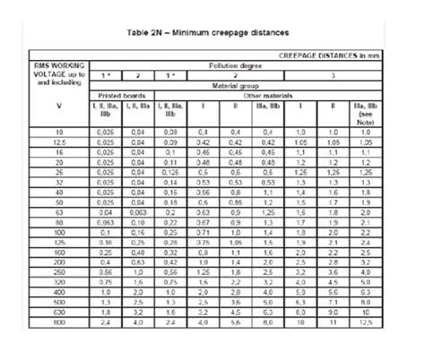
- IPC-2221B: Defines clearance requirements for voltages up to 500V.
- IEC 60950-1: Specifies clearance and creepage distances for IT equipment.
- UL 840: Outlines clearance and creepage requirements for insulation coordination.
The required clearance distances depend on the specific application and the standards applicable to the product.
Factors Influencing High Voltage Clearance
In addition to the factors mentioned earlier, high voltage PCB clearance is influenced by:
- Pollution degree: The amount of conductive pollution present in the environment affects the required clearance distances.
- Insulation type: The type of insulation used (functional, basic, supplementary, or reinforced) determines the necessary clearance.
- Altitude: Higher altitudes have lower air pressure, which reduces the dielectric strength of air and requires greater clearance distances.
Design Considerations for High Voltage PCBs
When designing high voltage PCBs, consider the following:
- Use appropriate insulation materials, such as FR-4 or ceramic substrates, to withstand the high voltages.
- Increase the thickness of the PCB to improve its dielectric strength and mechanical stability.
- Implement proper creepage and clearance distances based on the applicable standards and environmental conditions.
- Use conformal coatings or potting compounds to provide additional insulation and protection against environmental factors.

Comparing Low and High Voltage PCB Clearance
The main differences between low and high voltage PCB clearance requirements are:
- Clearance distances: High voltage PCBs require significantly larger clearance distances compared to low voltage PCBs.
- Insulation requirements: High voltage PCBs demand more robust insulation materials and techniques to prevent electrical breakdown.
- Environmental considerations: High voltage PCBs are more sensitive to environmental factors, such as pollution and altitude, which affect the required clearance distances.
- Safety considerations: High voltage PCBs pose a greater risk of electrical shock and fire, necessitating strict adherence to safety standards and design practices.
Best Practices for PCB Clearance Design
To ensure optimal PCB clearance design, follow these best practices:
- Understand the voltage levels and requirements of your specific application.
- Consult the relevant standards and guidelines for clearance and creepage distances.
- Consider the environmental conditions and pollution degree in which the PCB will operate.
- Use appropriate materials and manufacturing techniques to achieve the required clearance and insulation.
- Conduct thorough testing and verification to ensure the PCB meets the necessary clearance and safety requirements.
Frequently Asked Questions (FAQ)
- What is the difference between clearance and creepage distance?
-
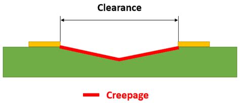
Clearance is the shortest distance through air between two conductive elements, while creepage is the shortest distance along the surface of the insulating material between two conductive elements.
-
How do I determine the appropriate clearance for my PCB?
-
The appropriate clearance depends on factors such as voltage level, PCB material, environmental conditions, and applicable standards. Consult the relevant standards and guidelines for your specific application.
-
Can I use the same clearance for low and high voltage PCBs?
-
No, high voltage PCBs require significantly larger clearance distances compared to low voltage PCBs due to the increased risk of electrical breakdown and arcing.
-
What happens if the clearance is insufficient on a PCB?
-
Insufficient clearance can lead to electrical shorts, arcing, insulation breakdown, and potentially dangerous conditions such as fire or electric shock.
-
How can I increase the clearance on a PCB with limited space?
- Strategies to increase clearance on a space-constrained PCB include using higher dielectric strength materials, increasing the PCB thickness, and implementing creative layout techniques such as staggered pads or air gaps.
Conclusion
PCB trace and pad clearance is a critical aspect of PCB design that ensures the reliability, safety, and functionality of electronic circuits. The clearance requirements differ significantly between low and high voltage PCBs, with the latter demanding greater distances and more robust insulation. By understanding the factors affecting clearance, consulting relevant standards, and following best design practices, engineers can create PCBs that meet the necessary clearance and safety requirements for their specific applications.

No responses yet