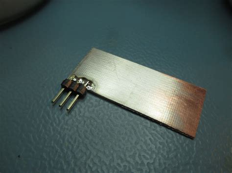
What is PCB Tinning?
PCB tinning is the process of applying a thin layer of solder to the exposed copper surfaces of a printed circuit board. This layer of solder, typically composed of a tin-lead alloy or lead-free alternatives, serves multiple purposes:
-
Protection against oxidation: Copper is prone to oxidation when exposed to air, which can lead to poor solderability and reduced electrical conductivity. The solder layer acts as a barrier, preventing oxidation and maintaining the integrity of the copper traces and pads.
-
Improved solderability: Tinned surfaces have better wetting properties, allowing the solder to flow more easily during the assembly process. This results in stronger and more reliable solder joints between components and the PCB.
-
Enhanced electrical conductivity: The solder layer provides a low-resistance electrical connection between components and the PCB, ensuring optimal signal integrity and power distribution.
Why is PCB Tinning Important?
PCB tinning plays a vital role in ensuring the quality, reliability, and longevity of electronic devices. Some of the key benefits of PCB tinning include:
-
Improved manufacturing process: Tinned PCBs are easier to assemble, as the solder layer facilitates the attachment of components to the board. This leads to faster production times and reduced assembly errors.
-
Increased reliability: By protecting the copper from oxidation and enhancing the solderability of the PCB, tinning contributes to the overall reliability of the electronic device. Well-tinned boards are less likely to experience solder joint failures or other issues related to poor solderability.
-
Extended product lifespan: The protective solder layer helps prevent the degradation of copper traces and pads over time, extending the lifespan of the PCB and the electronic device as a whole.
-
Compliance with industry standards: Many industries, such as aerospace, automotive, and medical, have strict requirements for PCB tinning to ensure the reliability and safety of electronic devices used in critical applications.

Methods of PCB Tinning
There are several methods used for PCB tinning, each with its own advantages and disadvantages. The choice of method depends on factors such as the size and complexity of the PCB, the desired thickness of the solder layer, and the available resources and equipment. Some of the most common PCB tinning methods include:
Hot Air Solder Leveling (HASL)
Hot Air Solder Leveling (HASL) is one of the most widely used PCB tinning methods. In this process, the PCB is first dipped into a molten solder bath, coating the exposed copper surfaces. The board is then passed through a series of hot air knives, which blow excess solder off the surface, leaving a thin, even layer of solder on the copper traces and pads.
Advantages of HASL:
– Cost-effective and suitable for high-volume production
– Provides good solderability and protection against oxidation
– Widely available and well-established in the industry
Disadvantages of HASL:
– Can result in uneven solder thickness, particularly on fine-pitch components
– The high temperatures involved may cause thermal stress on the PCB
– Not suitable for lead-free soldering processes
Immersion Silver (IAg)
Immersion Silver (IAg) is a lead-free PCB tinning method that involves dipping the board into a silver solution. The silver ions in the solution replace the copper atoms on the surface of the PCB, creating a thin, uniform layer of silver that protects the copper from oxidation and enhances solderability.
Advantages of IAg:
– Lead-free and RoHS compliant
– Provides excellent solderability and wetting properties
– Suitable for fine-pitch components and high-density PCBs
– Flat, planar surface finish
Disadvantages of IAg:
– More expensive than HASL
– Silver can tarnish over time, affecting solderability
– Not suitable for high-temperature applications
Electroless Nickel Immersion Gold (ENIG)
Electroless Nickel Immersion Gold (ENIG) is another lead-free PCB tinning method that involves depositing a thin layer of nickel onto the copper surfaces, followed by a thin layer of gold. The nickel layer provides a barrier against copper diffusion, while the gold layer protects the nickel from oxidation and enhances solderability.
Advantages of ENIG:
– Lead-free and RoHS compliant
– Excellent solderability and wetting properties
– Flat, planar surface finish
– Suitable for fine-pitch components and high-density PCBs
– Good shelf life and resistance to oxidation
Disadvantages of ENIG:
– More expensive than HASL and IAg
– The gold layer can be prone to “black pad” syndrome, which can lead to poor solder joint reliability
– Requires strict process control to ensure consistent quality
Comparison of PCB Tinning Methods
| Method | Advantages | Disadvantages |
|---|---|---|
| HASL | – Cost-effective – Good solderability – Widely available |
– Uneven solder thickness – Thermal stress on PCB – Not suitable for lead-free processes |
| IAg | – Lead-free and RoHS compliant – Excellent solderability – Suitable for fine-pitch components |
– More expensive than HASL – Silver can tarnish over time – Not suitable for high-temperature applications |
| ENIG | – Lead-free and RoHS compliant – Excellent solderability – Flat, planar surface finish – Good shelf life |
– More expensive than HASL and IAg – Prone to “black pad” syndrome – Requires strict process control |

Best Practices for PCB Tinning
To achieve the best results with PCB tinning, consider the following best practices:
-
Choose the appropriate tinning method based on your specific requirements, such as lead-free compliance, fine-pitch components, and budget constraints.
-
Ensure proper cleaning of the PCB prior to tinning to remove any contaminants or oxidation that may affect the quality of the solder layer.
-
Control the tinning process parameters, such as temperature, dwell time, and solder composition, to achieve consistent and reliable results.
-
Regularly maintain and calibrate the tinning equipment to ensure optimal performance and minimize process variations.
-
Conduct thorough inspections and quality checks on tinned PCBs to identify any defects or inconsistencies in the solder layer.
-
Store tinned PCBs in a controlled environment to prevent oxidation and contamination prior to the assembly process.

Frequently Asked Questions (FAQ)
-
What is the difference between lead-based and lead-free PCB tinning?
Lead-based tinning methods, such as HASL, use solder alloys containing lead, while lead-free methods, like IAg and ENIG, use alternative materials to comply with RoHS regulations. Lead-free tinning is becoming increasingly popular due to environmental and health concerns associated with lead. -
Can PCB tinning be done in-house, or should it be outsourced?
PCB tinning can be done in-house if you have the necessary equipment, expertise, and resources. However, outsourcing to a specialized PCB manufacturer is often more cost-effective and ensures consistent quality, particularly for high-volume production or complex designs. -
How does PCB tinning affect the assembly process?
Tinned PCBs have improved solderability and wetting properties, which facilitate the attachment of components to the board during the assembly process. This leads to faster production times, reduced assembly errors, and more reliable solder joints. -
What is the shelf life of tinned PCBs?
The shelf life of tinned PCBs depends on the tinning method and storage conditions. ENIG-tinned PCBs have a longer shelf life due to the protective gold layer, while IAg-tinned PCBs may tarnish over time, affecting solderability. In general, tinned PCBs should be stored in a controlled environment and used within a reasonable timeframe to ensure optimal performance. -
How can I inspect the quality of PCB tinning?
Visual inspection is the most common method for assessing the quality of PCB tinning. Look for a uniform, smooth, and continuous solder layer on the copper traces and pads. Solderability testing, such as the wetting balance test or the dip-and-look test, can also be used to evaluate the wetting properties and overall quality of the tinned surface.
Conclusion
PCB tinning is an essential process in the manufacturing of printed circuit boards, ensuring the reliability, longevity, and optimal performance of electronic devices. By understanding the importance of tinning, the various methods available, and best practices for achieving consistent results, you can make informed decisions when designing and manufacturing PCBs.
Whether you choose HASL, IAg, ENIG, or another tinning method, the key is to select the approach that best suits your specific requirements and to implement a robust quality control process to ensure the integrity of the tinned surfaces. By prioritizing PCB tinning and following industry best practices, you can create high-quality, reliable PCBs that will stand the test of time.
No responses yet