Understanding PCB Thickness
What is PCB Thickness?
PCB thickness refers to the measurement of the board’s height from top to bottom. It is typically expressed in either millimeters (mm) or mils (thousandths of an inch). The thickness of a PCB is determined by the number of layers it contains and the thickness of each individual layer.
Why Does PCB Thickness Matter?
The thickness of a PCB has a significant impact on several aspects of its performance and usability:
- Mechanical strength: Thicker PCBs are generally more robust and can withstand greater physical stress and vibration.
- Heat dissipation: Thicker boards can dissipate heat more effectively, which is crucial for high-power applications.
- Impedance control: The thickness of the board affects its impedance, which is essential for high-speed signal integrity.
- Manufacturing constraints: Thinner PCBs may be more challenging to manufacture and assemble, especially with fine-pitch components.
Standard PCB Thicknesses
Common PCB Thickness Options
PCB manufacturers offer a range of standard thicknesses to cater to different applications and requirements. The most common PCB thicknesses are:
| Thickness (mm) | Thickness (mils) | Layers |
|---|---|---|
| 0.4 | 16 | 1-2 |
| 0.6 | 24 | 1-2 |
| 0.8 | 32 | 2-4 |
| 1.0 | 39 | 4-6 |
| 1.2 | 47 | 4-8 |
| 1.6 | 63 | 6-10 |
| 2.0 | 79 | 8-12 |
| 2.4 | 94 | 10-14 |
Factors Influencing PCB Thickness Choice
When selecting the appropriate PCB thickness for your project, consider the following factors:
- Number of layers: More layers require a thicker board to accommodate the additional copper and insulation.
- Component requirements: Some components, such as connectors or heavy heatsinks, may require a thicker board for mechanical stability.
- Application environment: Harsh environments may necessitate thicker boards for increased durability.
- Manufacturing capabilities: Ensure that your chosen PCB manufacturer can reliably produce boards at your desired thickness.

PCB Thickness and Layer Count
Single-Layer PCBs
Single-layer PCBs are the simplest and most economical option, consisting of a single conductive layer on a dielectric substrate. These boards are typically 0.4mm to 0.6mm thick and are suitable for basic, low-density designs.
Double-Layer PCBs
Double-layer PCBs have conductive layers on both sides of the substrate, allowing for more complex routing and higher component density. These boards are commonly 0.6mm to 0.8mm thick and are widely used in consumer electronics and general-purpose applications.
Multi-Layer PCBs
Multi-layer PCBs consist of three or more conductive layers separated by insulating layers. As the number of layers increases, so does the thickness of the board. Multi-layer PCBs offer several advantages:
- Higher component density and more complex routing
- Improved signal integrity and noise reduction
- Better power distribution and heat dissipation
The table below shows the typical thickness ranges for multi-layer PCBs:
| Layers | Typical Thickness Range (mm) |
|---|---|
| 4 | 0.8 – 1.0 |
| 6 | 1.0 – 1.2 |
| 8 | 1.2 – 1.6 |
| 10 | 1.6 – 2.0 |
| 12 | 2.0 – 2.4 |

Advanced PCB Thickness Considerations
High-Frequency PCBs
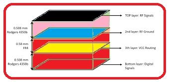
For high-frequency applications, such as RF and microwave circuits, the thickness of the PCB plays a critical role in signal integrity. In these cases, the dielectric constant and loss tangent of the substrate material, as well as the copper thickness, must be carefully controlled to maintain the desired impedance and minimize signal loss.
High-Power PCBs
In high-power applications, such as power electronics and automotive systems, thicker PCBs are often required to dissipate heat effectively and provide mechanical stability for heavy components. Copper thickness and the use of thermal management techniques, such as metal core PCBs or thermal vias, can also help improve heat dissipation.
Flexible PCBs
Flexible PCBs, made from thin, flexible substrates like polyimide, have thicknesses ranging from 0.1mm to 0.3mm. These thin, lightweight boards are ideal for applications requiring conformity to irregular shapes or where space is limited, such as wearable electronics and medical devices.

PCB Thickness Tolerances and Variations
Manufacturing Tolerances
PCB manufacturers specify thickness tolerances to account for variations in the production process. Typical thickness tolerances range from ±10% to ±20%, depending on the manufacturer and the specific PCB construction.
Copper Thickness Variations
The thickness of the copper layers on a PCB can also vary, affecting the overall thickness of the board. Standard copper thicknesses include:
| Copper Weight (oz) | Thickness (mm) |
|---|---|
| 0.5 | 0.017 |
| 1 | 0.035 |
| 2 | 0.070 |
| 3 | 0.105 |
Thicker copper layers can improve current carrying capacity and heat dissipation but may increase the overall cost of the PCB.
Frequently Asked Questions (FAQ)
-
Q: What is the most common PCB thickness?
A: The most common PCB thicknesses are 0.8mm, 1.0mm and 1.6mm, which are suitable for a wide range of applications and layer counts. -
Q: Can I use a thinner PCB to save cost?
A: While thinner PCBs may be less expensive, it’s essential to consider the specific requirements of your application, such as mechanical strength, heat dissipation, and signal integrity. Using a PCB that is too thin for your needs can lead to reliability issues and increased costs in the long run. -
Q: How does PCB thickness affect assembly?
A: Thinner PCBs can be more challenging to assemble, especially with fine-pitch components or heavy parts that require additional support. Thicker PCBs provide better mechanical stability and can simplify the assembly process. -
Q: What is the maximum number of layers for a PCB?
A: The maximum number of layers in a PCB is not strictly limited but is influenced by factors such as manufacturing capabilities, cost, and design complexity. PCBs with more than 14 layers are less common and may require specialized fabrication techniques. -
Q: How do I choose the right PCB thickness for my project?
A: When selecting the appropriate PCB thickness, consider factors such as the number of layers required, component sizes and weights, the application environment, and any specific electrical or thermal requirements. Consult with your PCB manufacturer for guidance on the best thickness for your specific project.
Conclusion
PCB thickness is a critical factor in the design and manufacturing of printed circuit boards, influencing mechanical strength, heat dissipation, signal integrity, and manufacturing feasibility. By understanding the standard PCB thicknesses and the factors that affect thickness choice, you can make informed decisions when designing your PCB projects.
When in doubt, consult with your PCB manufacturer to determine the optimal thickness for your specific application, taking into account your design requirements, the number of layers, and the intended operating environment. By selecting the appropriate PCB thickness, you can ensure the reliability, performance, and cost-effectiveness of your electronic products.
No responses yet