Introduction to PCB Surface Finish and Intermetallic Layers
Printed Circuit Boards (PCBs) are essential components in modern electronics, providing a platform for electrical components to be mounted and interconnected. The copper layer on a PCB is responsible for conducting electrical signals between components. However, exposed copper is susceptible to oxidation and corrosion, which can lead to decreased performance and reliability of the PCB. To protect the copper layer and ensure proper functionality, various surface finishes are applied to the PCB. One crucial aspect of these surface finishes is the formation of an intermetallic layer, which acts as a barrier between the copper and the environment.
In this article, we will delve into the importance of PCB surface finishes, with a particular focus on the role of the intermetallic layer in protecting the copper layer. We will explore the different types of surface finishes commonly used in the industry, their characteristics, and the formation and significance of the intermetallic layer in each case.
The Importance of PCB Surface Finishes
PCB surface finishes serve several critical functions in the manufacturing and assembly of electronic devices. Some of the key reasons for applying surface finishes to PCBs include:
- Protection against oxidation and corrosion
- Enhancing solderability
- Improving electrical conductivity
- Providing a suitable surface for component assembly
- Ensuring long-term reliability of the PCB
Without proper surface finishes, the exposed copper on a PCB would quickly oxidize, leading to decreased performance and potential failure of the electronic device. The intermetallic layer formed during the surface finishing process plays a vital role in preventing this degradation.

Common Types of PCB Surface Finishes
There are several types of surface finishes used in the PCB industry, each with its unique characteristics and benefits. Some of the most common surface finishes include:
1. Hot Air Solder Leveling (HASL)
HASL is one of the most widely used surface finishes in the PCB industry. In this process, the PCB is dipped into a molten solder bath, and then excess solder is removed using hot air knives. The resulting surface is relatively flat and provides excellent solderability.
Intermetallic Layer Formation in HASL
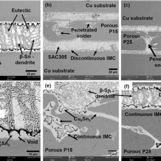
During the HASL process, an intermetallic layer is formed between the copper and the solder. This layer typically consists of copper-tin (Cu-Sn) intermetallic compounds, such as Cu6Sn5 and Cu3Sn. The formation of these intermetallic compounds is crucial for the adhesion and reliability of the solder joint.
2. Electroless Nickel Immersion Gold (ENIG)
ENIG is a popular surface finish for high-reliability applications. In this process, a layer of nickel is deposited onto the copper surface using an electroless plating method, followed by a thin layer of gold deposited through immersion.
Intermetallic Layer Formation in ENIG
In the ENIG process, an intermetallic layer is formed between the copper and the nickel. This layer is composed of copper-nickel (Cu-Ni) intermetallic compounds, such as Cu3Ni and CuNi. The formation of this intermetallic layer is essential for the adhesion and stability of the nickel layer on the copper surface.
3. Immersion Silver (IAg)
Immersion silver is a cost-effective surface finish that provides good solderability and electrical conductivity. In this process, a thin layer of silver is deposited onto the copper surface through an immersion plating method.
Intermetallic Layer Formation in IAg
During the immersion silver process, an intermetallic layer is formed between the copper and the silver. This layer consists of copper-silver (Cu-Ag) intermetallic compounds, such as Cu3Ag and CuAg. The formation of this intermetallic layer is crucial for the adhesion and stability of the silver layer on the copper surface.
4. Organic Solderability Preservative (OSP)
OSP is a surface finish that involves applying a thin, organic coating onto the copper surface to protect it from oxidation. This coating is designed to be easily removed during the soldering process, exposing the clean copper surface for soldering.
Intermetallic Layer Formation in OSP
In the OSP process, an intermetallic layer is not intentionally formed. However, during the soldering process, the OSP coating is removed, and the molten solder comes into direct contact with the copper surface. At this point, an intermetallic layer consisting of copper-tin (Cu-Sn) compounds is formed, similar to the HASL process.

The Significance of the Intermetallic Layer
The intermetallic layer formed during the surface finishing process plays a crucial role in the performance and reliability of the PCB. Some of the key functions of the intermetallic layer include:
-
Adhesion: The intermetallic layer ensures a strong bond between the copper and the surface finish, preventing delamination and improving the overall mechanical stability of the PCB.
-
Diffusion barrier: The intermetallic layer acts as a barrier, slowing down the diffusion of copper into the surface finish and vice versa. This helps maintain the integrity of the copper layer and prevents the formation of brittle intermetallic compounds that could lead to joint failure.
-
Corrosion resistance: The intermetallic layer provides an additional layer of protection against corrosion, as it is less susceptible to oxidation compared to pure copper.
-
Electrical conductivity: The intermetallic layer allows for efficient electrical conductivity between the copper layer and the surface finish, ensuring proper functionality of the PCB.

Factors Affecting Intermetallic Layer Formation
The formation of the intermetallic layer is influenced by several factors, including:
-
Temperature: Higher temperatures accelerate the formation of intermetallic compounds, as the increased energy allows for faster diffusion of atoms between the copper and the surface finish.
-
Time: Longer exposure to elevated temperatures leads to the growth of the intermetallic layer, as more time is available for diffusion and reaction between the copper and the surface finish.
-
Composition of the surface finish: The specific elements present in the surface finish can affect the type and growth rate of the intermetallic compounds formed.
-
Thickness of the surface finish: A thicker surface finish can slow down the growth of the intermetallic layer, as it takes longer for the copper atoms to diffuse through the surface finish.
Challenges and Considerations
While the intermetallic layer is essential for the performance and reliability of the PCB, its formation can also present some challenges:
-
Brittle intermetallic compounds: Some intermetallic compounds, such as Cu6Sn5, can be brittle and may lead to joint failure if they grow too thick.
-
Kirkendall voids: During the formation of the intermetallic layer, diffusion of atoms can lead to the formation of voids, known as Kirkendall voids. These voids can weaken the joint and lead to reliability issues.
-
Solderability: The growth of the intermetallic layer can affect the solderability of the PCB, as a thick intermetallic layer may hinder the wetting of the solder during the assembly process.
To mitigate these challenges, PCB manufacturers must carefully control the surface finishing process, including temperature, time, and the composition of the surface finish. Additionally, the choice of surface finish should be based on the specific requirements of the application, considering factors such as cost, performance, and reliability.
Future Trends and Developments
As the electronics industry continues to advance, there is an ongoing need for improved PCB surface finishes and intermetallic layer control. Some of the future trends and developments in this area include:
-
Novel surface finishes: Researchers are exploring new surface finish materials and processes that can provide enhanced protection, solderability, and electrical performance.
-
Nanostructured intermetallic layers: The use of nanotechnology in surface finishing processes may lead to the development of nanostructured intermetallic layers with improved mechanical and electrical properties.
-
Advanced process control: The implementation of advanced process control techniques, such as real-time monitoring and feedback control, can help optimize the formation of the intermetallic layer and minimize the occurrence of defects.
-
Simulation and modeling: The development of sophisticated simulation and modeling tools can aid in understanding and predicting the formation and growth of intermetallic layers, enabling better design and process optimization.
Conclusion
The intermetallic layer formed during the PCB surface finishing process plays a vital role in protecting the copper layer and ensuring the performance and reliability of the PCB. By understanding the formation, significance, and challenges associated with the intermetallic layer, PCB manufacturers can optimize their processes and select the most suitable surface finish for their specific applications.
As the electronics industry continues to evolve, ongoing research and development in the field of PCB surface finishes and intermetallic layer control will be crucial for meeting the ever-increasing demands for high-performance, reliable, and cost-effective electronic devices.
Frequently Asked Questions (FAQ)
-
What is an intermetallic layer in the context of PCB surface finishes?
An intermetallic layer is a thin layer of compounds formed between the copper layer of a PCB and the applied surface finish. This layer is created through the diffusion and reaction of atoms from the copper and the surface finish material, resulting in a new phase with distinct properties. -
Why is the formation of an intermetallic layer important for PCBs?
The intermetallic layer is crucial for several reasons: - It ensures a strong bond between the copper and the surface finish, preventing delamination.
- It acts as a diffusion barrier, slowing down the migration of copper into the surface finish and vice versa.
- It provides additional corrosion resistance to the copper layer.
-
It allows for efficient electrical conductivity between the copper and the surface finish.
-
What are some common types of PCB surface finishes that involve the formation of an intermetallic layer?
Some common PCB surface finishes that involve the formation of an intermetallic layer include: - Hot Air Solder Leveling (HASL): Forms copper-tin (Cu-Sn) intermetallic compounds.
- Electroless Nickel Immersion Gold (ENIG): Forms copper-nickel (Cu-Ni) intermetallic compounds.
-
Immersion Silver (IAg): Forms copper-silver (Cu-Ag) intermetallic compounds.
-
What factors influence the formation and growth of the intermetallic layer?
The formation and growth of the intermetallic layer are influenced by several factors: - Temperature: Higher temperatures accelerate the formation of intermetallic compounds.
- Time: Longer exposure to elevated temperatures leads to the growth of the intermetallic layer.
- Composition of the surface finish: The specific elements in the surface finish can affect the type and growth rate of the intermetallic compounds.
-
Thickness of the surface finish: A thicker surface finish can slow down the growth of the intermetallic layer.
-
What are some challenges associated with the formation of the intermetallic layer?
Some challenges associated with the formation of the intermetallic layer include: - Brittle intermetallic compounds: Some intermetallic compounds can be brittle, potentially leading to joint failure if they grow too thick.
- Kirkendall voids: Diffusion of atoms during intermetallic layer formation can lead to the formation of voids, which can weaken the joint.
- Solderability: A thick intermetallic layer may hinder the wetting of the solder during the assembly process.
| Surface Finish | Intermetallic Layer Composition | Key Characteristics |
|---|---|---|
| HASL | Cu-Sn (Cu6Sn5, Cu3Sn) | – Excellent solderability – Relatively flat surface |
| ENIG | Cu-Ni (Cu3Ni, CuNi) | – High reliability – Suitable for fine-pitch components |
| IAg | Cu-Ag (Cu3Ag, CuAg) | – Cost-effective – Good solderability and electrical conductivity |
| OSP | Cu-Sn (formed during soldering) | – Thin, organic coating – Easily removed during soldering |
No responses yet