Introduction to the PCB Supply Chain
The printed circuit board (PCB) is a critical component in virtually all modern electronic devices, from smartphones and laptops to medical equipment and aerospace systems. But have you ever stopped to think about the complex journey a PCB takes from initial design concept to finished product? In this article, we’ll take an in-depth look at the PCB supply chain, exploring each step of the process and the key players involved.
What is a PCB?
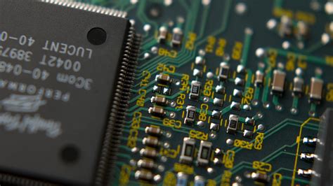
Before diving into the supply chain, let’s first define what a PCB is. A printed circuit board is a flat board made of insulating material, such as fiberglass, with conductive copper tracks printed onto its surface. These copper tracks form a complex pattern of electrical connections between the various components mounted on the board, such as resistors, capacitors, and integrated circuits (ICs). PCBs can be single-sided (with copper tracks on one side only), double-sided (with tracks on both sides), or multi-layered (with several layers of tracks sandwiched between insulating layers).
The Importance of the PCB Supply Chain
The PCB supply chain is a critical component of the global electronics industry. Without a reliable and efficient supply chain, electronics manufacturers would be unable to bring their products to market in a timely and cost-effective manner. The PCB supply chain involves a complex network of suppliers, manufacturers, and logistics providers, all working together to ensure that PCBs are designed, manufactured, and delivered to the end customer according to their specifications and timeline.
The PCB Design Process
The first step in the PCB supply chain is the design process. This is where the initial concept for the PCB is developed and refined into a detailed schematic and layout.
Schematic Design
The schematic design is the first step in the PCB design process. This involves creating a diagram that shows the electrical connections between the various components that will be mounted on the board. The schematic is typically created using electronic design automation (EDA) software, such as Altium Designer or KiCad.
Layout Design
Once the schematic is complete, the next step is to create the physical layout of the PCB. This involves determining the placement of components on the board and routing the copper tracks between them. The layout designer must take into account a variety of factors, such as signal integrity, power distribution, and thermal management, to ensure that the PCB will function properly once manufactured.
Design for Manufacturing (DFM)
Before finalizing the PCB design, it’s important to consider the manufacturability of the board. This is known as design for manufacturing (DFM), and it involves optimizing the design to ensure that it can be efficiently and reliably manufactured at scale. This may involve adjusting the placement of components, modifying the routing of tracks, or changing the materials used in the board.
PCB Manufacturing
Once the PCB design is finalized, the next step in the supply chain is manufacturing. This involves a series of processes to convert the digital design files into a physical board.
PCB Fabrication
The first step in PCB manufacturing is fabrication. This involves creating the bare board, which is the insulating substrate with the copper tracks printed onto its surface. The fabrication process typically involves the following steps:
- Material preparation: The insulating substrate material (e.g. fiberglass) is cut to size and cleaned.
- Copper deposition: A thin layer of copper is deposited onto the substrate using a process called electroplating.
- Photolithography: The copper layer is coated with a light-sensitive film, and the PCB design is transferred onto the film using a high-precision laser or UV light.
- Etching: The exposed copper is etched away using a chemical solution, leaving only the desired copper tracks on the board.
- Drilling: Holes are drilled into the board to accommodate through-hole components and vias (connections between layers).
- Solder mask application: A protective layer of solder mask is applied to the board to insulate the copper tracks and prevent short circuits.
- Silkscreen printing: Text and symbols are printed onto the board using a silkscreen process to aid in assembly and identification of components.
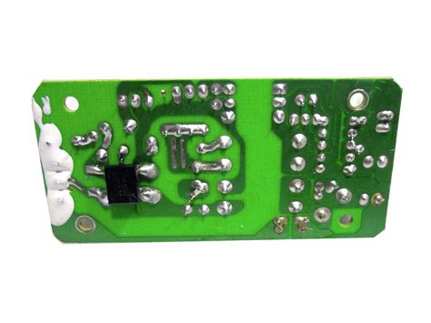
PCB Assembly
Once the bare board is fabricated, the next step is assembly. This involves mounting the various electronic components onto the board and soldering them in place. There are two main methods of PCB assembly:
- Through-hole assembly: Components with long leads are inserted into holes drilled in the board and soldered in place on the opposite side.
- Surface-mount assembly: Components with small metal pads are placed onto corresponding pads on the board and soldered in place using a reflow oven.
PCB assembly can be done manually by skilled technicians or automatically using pick-and-place machines and reflow ovens.
Quality Control and Testing
After assembly, each PCB undergoes rigorous quality control and testing to ensure that it meets the required specifications and functions properly. This may involve visual inspection, automated optical inspection (AOI), X-ray inspection, and functional testing.

PCB Logistics and Distribution
Once the PCBs are manufactured and tested, they need to be packaged and shipped to the customer or the next stage in the manufacturing process (e.g. final product assembly). This involves a complex network of logistics providers and distribution centers.
Packaging and Labeling
PCBs are typically packaged in anti-static bags or boxes to protect them from damage during shipping. Each package is labeled with a unique identifier, such as a barcode or QR code, to enable tracking and traceability throughout the supply chain.
Shipping and Distribution
PCBs are shipped using a variety of methods, depending on the size of the order, the distance to the customer, and the required delivery time. Common shipping methods include:
- Air freight: For high-priority or time-sensitive orders
- Ocean freight: For large orders or less time-sensitive shipments
- Ground transportation: For domestic or regional shipments
PCBs are often shipped to distribution centers or warehouses before being delivered to the end customer. This allows for more efficient inventory management and faster delivery times.
Customs and Regulations
When shipping PCBs internationally, there are a variety of customs and regulatory requirements that must be met. These may include:
- Export licenses and permits
- Tariffs and duties
- Hazardous materials (HAZMAT) regulations for certain components or materials
- Conflict minerals reporting requirements
- RoHS (Restriction of Hazardous Substances) and REACH (Registration, Evaluation, Authorization and Restriction of Chemicals) compliance
Navigating these requirements can be complex and time-consuming, which is why many electronics manufacturers rely on specialized logistics providers with expertise in international trade compliance.
Key Players in the PCB Supply Chain
The PCB supply chain involves a complex network of suppliers, manufacturers, and service providers. Some of the key players include:
PCB Design Software Providers
Companies that provide electronic design automation (EDA) software for schematic capture, layout design, and simulation. Examples include:
- Altium
- Cadence Design Systems
- Mentor Graphics (now part of Siemens)
- Zuken
PCB Manufacturers
Companies that specialize in the fabrication and assembly of PCBs. These can range from small, specialized shops to large, global manufacturers. Examples include:
- Foxconn
- Jabil Circuit
- Sanmina
- TTM Technologies
Electronic Component Suppliers
Companies that provide the various electronic components that are mounted onto PCBs, such as resistors, capacitors, and integrated circuits (ICs). Examples include:
- Arrow Electronics
- Avnet
- Digi-Key Electronics
- Mouser Electronics
Logistics Providers
Companies that specialize in the packaging, shipping, and distribution of PCBs and other electronic components. Examples include:
- DHL
- FedEx
- UPS
- DB Schenker
Testing and Inspection Equipment Providers
Companies that provide equipment and software for quality control and testing of PCBs, such as automated optical inspection (AOI) machines and X-ray inspection systems. Examples include:
- Agilent Technologies
- Keysight Technologies
- Teradyne
- Yxlon International
Challenges and Trends in the PCB Supply Chain
The PCB supply chain is constantly evolving to meet the changing needs of the electronics industry. Some of the key challenges and trends include:
Miniaturization and High Density Interconnect (HDI)
As electronic devices become smaller and more complex, there is a growing demand for PCBs with higher density interconnects and smaller feature sizes. This requires advanced manufacturing capabilities and close collaboration between design and manufacturing teams.
Supply Chain Disruptions
The PCB supply chain is vulnerable to disruptions caused by natural disasters, geopolitical events, and other unforeseen circumstances. The COVID-19 pandemic, for example, has caused significant disruptions to the global electronics supply chain, highlighting the need for greater resilience and agility.
Environmental and Sustainability Concerns
There is growing pressure on the electronics industry to reduce its environmental impact and improve sustainability throughout the supply chain. This includes reducing the use of hazardous substances, improving energy efficiency, and promoting recycling and reuse of materials.
Skilled Labor Shortages
The PCB industry relies on skilled technicians and engineers for design, manufacturing, and testing. However, many companies are facing shortages of skilled labor, particularly in regions with high labor costs. This is driving a trend towards automation and the use of advanced manufacturing technologies, such as 3D printing and robotics.
The Future of the PCB Supply Chain
As the electronics industry continues to evolve, so too will the PCB supply chain. Some of the key trends and developments to watch include:
Industry 4.0 and Smart Manufacturing
The adoption of Industry 4.0 technologies, such as the Internet of Things (IoT), big data analytics, and artificial intelligence (AI), is transforming the PCB supply chain. These technologies enable greater automation, visibility, and optimization throughout the manufacturing process, from design to delivery.
5G and the Internet of Things (IoT)
The rollout of 5G networks and the growing adoption of IoT devices are driving demand for new types of PCBs, such as high-frequency and flexible PCBs. This is creating new opportunities and challenges for PCB manufacturers and suppliers.
Circular Economy and Sustainability
There is growing interest in the concept of a circular economy, in which resources are kept in use for as long as possible through reuse, recycling, and remanufacturing. This is driving the development of new technologies and business models for PCB manufacturing, such as closed-loop recycling and product-as-a-service.
Reshoring and Regionalization
The COVID-19 pandemic has highlighted the risks of relying on a highly globalized supply chain, particularly for critical components such as PCBs. This is driving a trend towards reshoring and regionalization of PCB manufacturing, with companies looking to reduce their dependence on offshore suppliers and improve supply chain resilience.
Conclusion
The PCB supply chain is a complex and dynamic ecosystem that plays a critical role in the global electronics industry. From design and manufacturing to logistics and distribution, each stage of the supply chain involves a network of suppliers, service providers, and customers working together to bring new products to market.
As the industry continues to evolve, driven by trends such as miniaturization, sustainability, and digitalization, the PCB supply chain will need to adapt and innovate to meet new challenges and opportunities. By understanding the key players, processes, and trends shaping the industry, companies can position themselves for success in the years ahead.
FAQ
What is a PCB and why is it important?
A PCB, or printed circuit board, is a essential component in virtually all electronic devices. It provides the electrical connections and mechanical support for the various components that make up the device. Without PCBs, modern electronics would not be possible.
What are the key steps in the PCB manufacturing process?
The PCB manufacturing process typically involves the following steps:
- Design: Creating the schematic and layout files for the PCB
- Fabrication: Creating the bare board by printing and etching the copper tracks onto the insulating substrate
- Assembly: Mounting and soldering the electronic components onto the board
- Testing and Inspection: Verifying that the PCB meets the required specifications and functions properly
What are some of the key challenges facing the PCB supply chain?
Some of the key challenges facing the PCB supply chain include:
- Miniaturization and increasing complexity of PCB designs
- Supply chain disruptions caused by natural disasters, geopolitical events, and other unforeseen circumstances
- Environmental and sustainability concerns, such as the use of hazardous substances and the need for improved recycling and reuse of materials
- Skilled labor shortages, particularly in regions with high labor costs
What are some of the key trends shaping the future of the PCB supply chain?
Some of the key trends shaping the future of the PCB supply chain include:
- The adoption of Industry 4.0 technologies, such as IoT, big data analytics, and AI
- The growing demand for 5G and IoT-enabled devices, which require new types of PCBs
- The shift towards a circular economy and increased focus on sustainability
- The trend towards reshoring and regionalization of PCB manufacturing to improve supply chain resilience
How can companies navigate the complexities of the PCB supply chain?
To navigate the complexities of the PCB supply chain, companies can:
- Develop strong relationships with key suppliers and service providers
- Invest in advanced manufacturing technologies and processes to improve efficiency and quality
- Implement robust supply chain risk management and business continuity planning
- Stay up-to-date on the latest industry trends and regulations
- Foster a culture of continuous improvement and innovation throughout the organization
By understanding the key players, processes, and trends shaping the PCB supply chain, companies can position themselves for success in an increasingly complex and dynamic industry.
No responses yet