Introduction to PCB Stackup and Impedance Control
Printed Circuit Board (PCB) stackup refers to the arrangement of copper layers and dielectric materials that make up a PCB. The stackup design plays a crucial role in determining the electrical performance, signal integrity, and manufacturability of the PCB. One of the key aspects of PCB stackup design is impedance control, which involves managing the characteristic impedance of transmission lines to ensure proper signal propagation and minimize reflections.
In high-speed digital designs, it is essential to maintain consistent impedance throughout the signal path to avoid signal integrity issues such as reflections, crosstalk, and electromagnetic interference (EMI). Impedance control is achieved by carefully selecting the appropriate dielectric materials, copper weights, and trace geometries in the PCB stackup.
Importance of PCB Stackup and Impedance Control
- Signal Integrity: Proper impedance control helps maintain signal integrity by minimizing reflections and ensuring clean, undistorted signals.
- EMI Reduction: Consistent impedance reduces electromagnetic interference (EMI) by preventing unwanted radiation and coupling between signal traces.
- High-Speed Performance: Impedance-controlled PCBs are essential for high-speed digital designs, enabling faster data rates and cleaner signal transitions.
- Reliability: A well-designed PCB stackup with controlled impedance enhances the overall reliability of the electronic system.
Factors Affecting PCB Stackup Impedance
Several factors influence the characteristic impedance of a PCB stackup. Understanding these factors is crucial for designing a stackup that meets the desired impedance requirements.
1. Dielectric Material Properties
The dielectric material properties, such as dielectric constant (Dk) and dissipation factor (Df), significantly impact the impedance of a PCB stackup. The dielectric constant determines the capacitance between the signal trace and the reference plane, while the dissipation factor affects the loss tangent of the material.
Common dielectric materials used in PCB fabrication include:
| Material | Dielectric Constant (Dk) | Dissipation Factor (Df) |
|---|---|---|
| FR-4 | 4.2 – 4.5 | 0.02 – 0.03 |
| Rogers 4350B | 3.48 | 0.0037 |
| Isola 370HR | 3.70 | 0.0170 |
| Nelco N4000-6 | 3.90 | 0.0140 |
2. Copper Thickness and Trace Geometry
The thickness of the copper layers and the geometry of the signal traces also affect the impedance of the PCB stackup. Thicker copper layers result in lower impedance, while thinner layers lead to higher impedance. The trace width and spacing between traces also contribute to the overall impedance.
Common copper weights used in PCB fabrication include:
| Copper Weight | Thickness (oz) | Thickness (μm) |
|---|---|---|
| 0.5 oz | 0.0007 | 17.5 |
| 1 oz | 0.0014 | 35 |
| 2 oz | 0.0028 | 70 |
| 3 oz | 0.0042 | 105 |
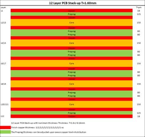
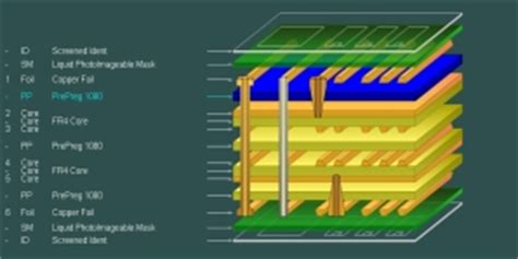
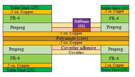
3. Stackup Configuration
The arrangement of copper layers and dielectric materials in the PCB stackup influences the impedance. The number of layers, their order, and the spacing between them all contribute to the characteristic impedance of the transmission lines.
Common stackup configurations include:
- 2-layer PCB: Signal layer and ground layer
- 4-layer PCB: Signal layer, ground layer, power layer, signal layer
- 6-layer PCB: Signal layer, ground layer, signal layer, power layer, ground layer, signal layer
- 8-layer PCB: Multiple signal, ground, and power layers
Calculating PCB Stackup Impedance
To calculate the characteristic impedance of a PCB stackup, several methods can be employed, including analytical calculations, simulation tools, and the use of impedance calculators.
1. Analytical Calculations
Analytical calculations involve using mathematical formulas to determine the characteristic impedance based on the properties of the dielectric material, copper thickness, and trace geometry. The most common formula for calculating the impedance of a microstrip transmission line is:
Z0 = (87 / sqrt(Er + 1.41)) * ln(5.98 * h / (0.8 * w + t))
Where:
– Z0 is the characteristic impedance in ohms
– Er is the dielectric constant of the substrate material
– h is the height of the dielectric between the signal trace and the reference plane
– w is the width of the signal trace
– t is the thickness of the copper trace
For stripline transmission lines, the following formula can be used:
Z0 = (60 / sqrt(Er)) * ln(4 * h / (0.67 * (0.8 * w + t)))
2. Simulation Tools
Simulation tools, such as electromagnetic field solvers, can be used to accurately model and analyze the impedance of a PCB stackup. These tools take into account the complex interactions between the signal traces, dielectric materials, and reference planes, providing detailed impedance profiles and helping optimize the stackup design.
Popular simulation tools for PCB stackup impedance analysis include:
- Ansys HFSS
- Keysight ADS
- Cadence Allegro PCB SI
- Altium Designer
3. Impedance Calculators
Impedance calculators are software tools that simplify the process of calculating the characteristic impedance of a PCB stackup. These calculators typically require inputs such as the dielectric material properties, copper weights, trace dimensions, and stackup configuration. They then provide the estimated impedance values based on the provided inputs.
Some popular impedance calculators include:
- Saturn PCB Toolkit
- EEWeb PCB Impedance Calculator
- Polar Instruments Si9000e Impedance Calculator
- PCB Symphony Impedance Calculator

PCB Stackup Design Considerations for Impedance Control
When designing a PCB stackup for impedance control, several key considerations should be taken into account to ensure optimal performance and manufacturability.
1. Material Selection
Choosing the appropriate dielectric materials is crucial for achieving the desired impedance and minimizing signal loss. Factors to consider when selecting materials include:
- Dielectric constant (Dk) stability over frequency and temperature
- Dissipation factor (Df) for low-loss performance
- Thermal stability and mechanical properties
- Cost and availability
2. Copper Weight and Trace Geometry
The choice of copper weight and trace geometry should be based on the impedance requirements, current-carrying capacity, and manufacturing capabilities. Consider the following:
- Thicker copper weights for lower impedance and higher current-carrying capacity
- Thinner copper weights for higher impedance and finer trace geometries
- Trace width and spacing for impedance control and crosstalk reduction
- Manufacturability and cost implications of chosen copper weights and trace geometries
3. Reference Plane Placement
Proper placement of reference planes (ground and power) is essential for maintaining consistent impedance and minimizing signal integrity issues. Consider the following:
- Placing reference planes close to signal layers to reduce loop inductance
- Using continuous reference planes to provide uninterrupted return paths
- Avoiding split reference planes, which can cause impedance discontinuities
- Utilizing stitching vias to connect reference planes and minimize EMI
4. Via Design and Placement
Vias play a critical role in maintaining impedance continuity and minimizing signal degradation. Consider the following:
- Minimizing via stubs to reduce impedance discontinuities and reflections
- Using appropriate via sizes and pad geometries for impedance matching
- Placing vias strategically to minimize crosstalk and signal coupling
- Employing via shielding techniques, such as ground vias, for sensitive signals
5. Signal Layer Arrangement
The arrangement of signal layers in the PCB stackup can impact impedance control and signal integrity. Consider the following:
- Alternating signal layers with reference planes to provide continuous return paths
- Grouping similar signal types (e.g., high-speed, low-speed, analog) on separate layers
- Minimizing crosstalk by separating sensitive signals from noisy signals
- Utilizing differential pair routing for high-speed signals
PCB Stackup Impedance Verification and Testing
After designing the PCB stackup and completing the layout, it is essential to verify the impedance characteristics and perform testing to ensure compliance with the desired specifications.
1. Impedance Verification Methods
Several methods can be used to verify the impedance of a PCB stackup:
- Time Domain Reflectometry (TDR): TDR measures the impedance profile along a transmission line by sending a fast-rising step signal and analyzing the reflections.
- Time Domain Transmission (TDT): TDT measures the impedance by analyzing the transmitted signal through a transmission line.
- Vector Network Analyzer (VNA): VNA measures the scattering parameters (S-parameters) of a PCB, providing information about impedance, return loss, and insertion loss.
2. Manufacturing Coupon Testing
Manufacturing coupons are small PCB sections that are fabricated alongside the main PCB panel. These coupons contain impedance test structures that can be used to verify the impedance characteristics of the manufactured PCB. By testing the coupons, manufacturers can ensure that the PCB stackup meets the specified impedance requirements.
3. Acceptance Criteria and Tolerances
When verifying the impedance of a PCB stackup, it is important to establish acceptance criteria and tolerances. The acceptance criteria should be based on the design requirements and the specific application of the PCB. Common tolerances for impedance control are:
- ±10% for general-purpose designs
- ±5% for high-speed designs
- ±2% for ultra-high-speed and high-precision designs
Frequently Asked Questions (FAQ)
- Q: What is the difference between microstrip and stripline transmission lines?
A: Microstrip transmission lines have a signal trace on one side of the dielectric and a reference plane on the other side, while stripline transmission lines have signal traces embedded between two reference planes in the dielectric layer. - Q: How does the dielectric constant affect the impedance of a PCB stackup?
A: A higher dielectric constant results in lower impedance, while a lower dielectric constant leads to higher impedance. The dielectric constant determines the capacitance between the signal trace and the reference plane. - Q: What is the importance of reference plane placement in PCB stackup design?
A: Proper reference plane placement is crucial for maintaining consistent impedance, providing uninterrupted return paths, and minimizing signal integrity issues such as EMI and crosstalk. - Q: How can I minimize impedance discontinuities caused by vias?
A: To minimize impedance discontinuities caused by vias, you can: - Use appropriate via sizes and pad geometries for impedance matching
- Minimize via stubs by using blind or buried vias
- Place vias strategically to reduce signal coupling and crosstalk
- Employ via shielding techniques, such as ground vias, for sensitive signals
- Q: What are the common methods for verifying the impedance of a manufactured PCB?
A: Common methods for verifying the impedance of a manufactured PCB include: - Time Domain Reflectometry (TDR)
- Time Domain Transmission (TDT)
- Vector Network Analyzer (VNA)
- Manufacturing coupon testing
Conclusion
PCB stackup impedance control is a critical aspect of high-speed digital design, ensuring signal integrity, reducing EMI, and enhancing the overall reliability of electronic systems. By understanding the factors affecting PCB stackup impedance, such as dielectric material properties, copper thickness, trace geometry, and stackup configuration, designers can create well-controlled impedance structures.
Calculating PCB stackup impedance involves analytical calculations, simulation tools, and the use of impedance calculators. When designing a PCB stackup for impedance control, key considerations include material selection, copper weight and trace geometry, reference plane placement, via design and placement, and signal layer arrangement.
Verifying the impedance characteristics of a manufactured PCB is essential to ensure compliance with the desired specifications. Methods such as TDR, TDT, VNA, and manufacturing coupon testing can be employed for impedance verification.
By following best practices and guidelines for PCB stackup design and impedance control, designers can create reliable, high-performance electronic systems that meet the ever-increasing demands of modern applications.
No responses yet