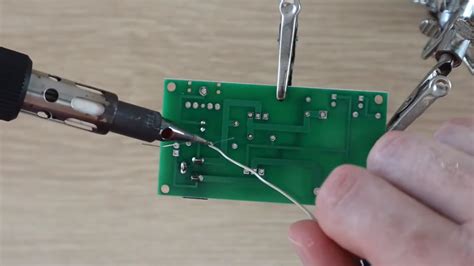
What is PCB Soldering?
PCB soldering is the process of joining electronic components to a printed circuit board (PCB) using solder, a fusible metal alloy. Soldering creates a permanent electrical and mechanical connection between the component leads and the PCB’s copper pads or through-holes. This technique is essential for assembling and repairing electronic devices, from simple hobby projects to complex industrial applications.
Types of PCB Soldering
There are two primary types of PCB soldering:
-
Through-hole soldering: Components with long leads are inserted through holes drilled in the PCB, and the leads are soldered to pads on the opposite side of the board.
-
Surface-mount soldering: Components with small leads or terminations are soldered directly onto pads on the surface of the PCB.
Tools and Materials Required for PCB Soldering
To perform PCB soldering effectively, you’ll need the following tools and materials:
Soldering Iron
A soldering iron is a hand tool that heats up and melts solder to create a connection between components and the PCB. When choosing a soldering iron, consider the following factors:
- Wattage: A soldering iron with adjustable temperature control and a power rating between 20-60 watts is suitable for most PCB soldering tasks.
- Tip type: Different tip shapes and sizes are available for various soldering applications. Common tip types include conical, chisel, and beveled tips.
Solder
Solder is a metal alloy that melts at a relatively low temperature and creates a strong bond between components and the PCB. The most common types of solder used in electronics are:
- Lead-based solder: Typically a 60/40 tin-lead alloy, known for its ease of use and low melting point. However, lead-based solder is being phased out due to environmental and health concerns.
- Lead-free solder: Usually consists of tin, copper, and silver, with a slightly higher melting point than lead-based solder. Lead-free solder is becoming the standard in the electronics industry.
When selecting solder, also consider the diameter of the solder wire. A thinner wire (e.g., 0.5mm) is better for precise work and smaller components, while a thicker wire (e.g., 1.0mm) is more suitable for larger components and connections.
Flux
Flux is a chemical cleaning agent that removes oxides from metal surfaces, allowing the solder to flow and bond more easily. Flux comes in various forms, such as:
- Rosin core solder wire: Solder wire with a built-in flux core, which is the most convenient option for most PCB soldering tasks.
- Flux pen or bottle: Liquid flux that can be applied directly to the soldering area for more precise control or when using solid solder wire.
Other Tools and Accessories
- Soldering iron stand: Safely holds the soldering iron when not in use and includes a sponge or brass wool for cleaning the tip.
- Solder wick or desoldering braid: A braided copper wire used to remove excess solder from joints or correct soldering mistakes.
- Tweezers: Help position and hold small components during soldering.
- Wire cutters: Used to trim component leads after soldering.
- Isopropyl alcohol and cotton swabs: For cleaning the PCB before and after soldering.
- Safety glasses and ventilation: Protect your eyes from solder splashes and ensure adequate ventilation to minimize exposure to soldering fumes.

PCB Soldering Techniques
Through-Hole Soldering
- Prepare the components and PCB:
- Bend the component leads to fit through the designated holes in the PCB.
- Insert the component leads through the holes, ensuring the component is seated flush against the PCB.
-
Bend the leads slightly outward on the opposite side of the PCB to hold the component in place.
-
Clean and tin the soldering iron tip:
- Wipe the hot soldering iron tip on a damp sponge or brass wool to remove any oxide buildup.
-
Apply a small amount of solder to the tip to ensure good heat transfer (called “tinning”).
-
Apply heat and solder:
- Touch the soldering iron tip to the component lead and the PCB pad simultaneously.
- Apply solder to the joint, allowing it to melt and flow around the lead and pad. Use just enough solder to create a concave fillet around the lead.
-
Remove the solder wire and the soldering iron, and let the joint cool for a few seconds.
-
Inspect the soldered joint:
- A good solder joint should be shiny, smooth, and concave, with the solder adhering well to both the lead and the pad.
-
If the joint appears dull, bulky, or has a convex shape, it may indicate a poor connection and require reheating or removal.
-
Trim the excess leads:
- Use wire cutters to trim the component leads close to the soldered joint, leaving about 1-2mm of the lead protruding.
Surface-Mount Soldering
- Apply solder paste (if using):
-
If the PCB doesn’t have pre-applied solder paste, use a syringe or stencil to apply a small amount of solder paste to the pads.
-
Position the components:
- Use tweezers to place the surface-mount components on their designated pads, ensuring proper alignment and orientation.
-
If the PCB has a solder mask, align the component terminations with the openings in the mask.
-
Preheat the PCB (optional):
-
For temperature-sensitive components or larger PCBs, use a preheating method (e.g., a hot plate or reflow oven) to gradually raise the PCB temperature and minimize thermal shock.
-
Apply heat and solder:
- Touch the soldering iron tip to the component termination and the PCB pad simultaneously.
- If using solder wire, apply a small amount of solder to the joint, allowing it to melt and flow between the termination and pad.
- If using solder paste, the heat from the soldering iron will melt the paste and create the joint.
-
Remove the soldering iron and let the joint cool for a few seconds.
-
Inspect the soldered joint:
- A good surface-mount solder joint should have a concave meniscus shape, with the solder wetting both the component termination and the PCB pad evenly.
- Check for any bridging (unwanted solder connections) between adjacent pads or pins, and remove excess solder with solder wick if necessary.

Common PCB Soldering Problems and Solutions
- Cold solder joint:
- Problem: A cold solder joint appears dull, grainy, or bulky and may have a poor electrical connection.
- Causes: Insufficient heat, improper solder flow, or movement during cooling.
-
Solution: Reheat the joint with the soldering iron, apply additional solder if needed, and ensure the joint cools undisturbed.
-
Bridging:
- Problem: Unwanted solder connections between adjacent pads or pins.
- Causes: Excessive solder application or improper soldering technique.
-
Solution: Use solder wick to remove the excess solder and reheat the joint if necessary.
-
Solder balls or splatter:
- Problem: Small solder balls or splatter on the PCB surface.
- Causes: Excessive solder, high soldering iron temperature, or rapid removal of the iron from the joint.
-
Solution: Remove solder balls with tweezers or solder wick, and adjust soldering technique to minimize splatter.
-
Overheated components:
- Problem: Components may be damaged by excessive heat during soldering.
- Causes: Prolonged soldering time or high soldering iron temperature.
-
Solution: Use the appropriate soldering iron temperature, minimize soldering time, and consider using a heat sink on sensitive components.
-
Insufficient wetting:
- Problem: Solder does not adhere well to the component lead or PCB pad.
- Causes: Insufficient flux, oxidized surfaces, or incorrect soldering temperature.
- Solution: Clean the surfaces with isopropyl alcohol, use fresh solder and flux, and ensure the soldering iron temperature is appropriate for the solder type.

PCB Soldering Safety Considerations
-
Eye protection: Wear safety glasses to protect your eyes from solder splashes or flying debris.
-
Ventilation: Ensure adequate ventilation or use a fume extractor to minimize exposure to soldering fumes, which may contain harmful chemicals.
-
Burn prevention: Be cautious when handling the hot soldering iron, and always place it in a soldering iron stand when not in use. Avoid touching the soldered joints until they have cooled down.
-
Ingestion and inhalation: Avoid eating, drinking, or smoking while soldering, and wash your hands thoroughly after soldering to prevent ingestion of lead or other harmful substances.
-
Proper disposal: Dispose of solder waste, used solder wick, and other soldering byproducts in accordance with local environmental regulations.
FAQ
-
What is the difference between lead-based and lead-free solder?
Lead-based solder contains a 60/40 tin-lead alloy, while lead-free solder typically consists of tin, copper, and silver. Lead-based solder has a lower melting point and is easier to work with, but it is being phased out due to environmental and health concerns. Lead-free solder has a slightly higher melting point and may require different soldering techniques. -
How do I choose the right soldering iron tip for my project?
Consider the size and type of components you’ll be soldering, as well as the PCB’s design. For through-hole components, a chisel or beveled tip works well. For surface-mount components, a fine conical or chisel tip is more suitable. Always choose a tip that provides good heat transfer and allows easy access to the soldering area. -
Can I reuse solder wick?
While it is possible to reuse solder wick, it is generally not recommended. Solder wick becomes less effective at absorbing solder after each use, and it may introduce contaminants to the soldering area. It’s best to use fresh solder wick for each desoldering task to ensure optimal results. -
How do I clean my PCB after soldering?
Use isopropyl alcohol (90% or higher) and a lint-free cloth or cotton swabs to clean the PCB after soldering. This helps remove flux residue, which can be corrosive and may cause long-term damage to the PCB. Be sure to clean the PCB gently to avoid damaging the components or solder joints. -
What should I do if I accidentally bridge two pins or pads while soldering?
If you notice a solder bridge between two pins or pads, use solder wick to remove the excess solder. Place the solder wick on the bridge and apply the soldering iron tip to the wick. The solder will be drawn up into the wick by capillary action. Repeat the process until the bridge is removed, and then inspect the joint to ensure proper separation between the pins or pads.
Conclusion
PCB soldering is a critical skill for anyone involved in electronic assembly or repair. By understanding the tools, techniques, and safety considerations involved in PCB soldering, you can create reliable and efficient electronic connections. Remember to practice proper soldering techniques, use the appropriate tools and materials, and always prioritize safety when working with soldering equipment. With patience and practice, you’ll be able to master the art of PCB soldering and bring your electronic projects to life.
No responses yet