Importance of Proper PCB Soldering
Proper PCB soldering is essential for several reasons:
- Reliability: Well-soldered connections ensure that the electronic device functions reliably and without interruptions.
- Durability: Properly soldered joints can withstand mechanical stress and vibrations, increasing the device’s lifespan.
- Performance: Good soldering techniques minimize electrical resistance and ensure optimal signal transmission, resulting in better device performance.
- Safety: Poorly soldered joints can lead to short circuits, overheating, and potential fire hazards.
Common PCB Soldering Problems
1. Cold Solder Joints
Cold solder joints occur when the solder does not melt completely or when the solder joint is disturbed during the cooling process. Characteristics of cold solder joints include:
- Dull, grainy, or pitted appearance
- Cracked or incomplete solder fillets
- High electrical resistance
To avoid cold solder joints:
- Ensure that the soldering iron is at the correct temperature
- Apply the soldering iron and solder simultaneously to the joint
- Keep the soldering iron in contact with the joint until the solder flows properly
- Avoid moving the joint until the solder has solidified
2. Bridging
Bridging occurs when solder inadvertently connects two or more adjacent pads or traces on the PCB. It can lead to short circuits and device malfunction. Causes of bridging include:
- Excessive solder application
- Improper soldering iron tip size or shape
- Insufficient spacing between pads or traces
To prevent bridging:
- Use the appropriate amount of solder
- Select the correct soldering iron tip for the job
- Ensure adequate spacing between pads and traces during PCB design
- Use a solder wick or desoldering pump to remove excess solder
3. Insufficient Solder
Insufficient solder can result in weak or unreliable connections. It may occur due to:
- Inadequate solder application
- Incorrect soldering iron temperature
- Contaminated or oxidized surfaces
To avoid insufficient solder:
- Apply enough solder to create a concave fillet between the component lead and pad
- Maintain the correct soldering iron temperature
- Clean and prep surfaces before soldering
4. Excessive Solder
Excessive solder application can lead to bridging, increased joint size, and difficulty in inspection. It may happen due to:
- Overfeeding solder
- Incorrect soldering iron tip size
- Prolonged soldering time
To prevent excessive solder:
- Apply solder in controlled amounts
- Use the appropriate soldering iron tip size
- Limit soldering time to prevent heat buildup
5. Tombstoning
Tombstoning, also known as drawbridging, occurs when a surface-mount component stands up on one end during soldering. It is caused by an imbalance in the solder surface tension on the component’s pads. Factors contributing to tombstoning include:
- Uneven heating of the pads
- Misalignment of the component
- Differences in pad sizes or
shapes
To mitigate tombstoning:
- Ensure even heating of the pads
- Align components properly before soldering
- Design pads with similar sizes and shapes
- Use solder paste with a balanced flux composition
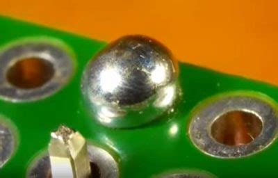
6. Solder Balls
Solder balls are small spherical balls of solder that can form and detach from the solder joint. They can cause short circuits if they come into contact with other components or traces. Solder balls can result from:
- Excessive solder application
- High soldering iron temperature
- Contaminated or oxidized surfaces
To avoid solder balls:
- Apply solder in controlled amounts
- Maintain the correct soldering iron temperature
- Clean and prep surfaces before soldering
- Use a fine-tipped soldering iron for precise control
7. Solder Spikes
Solder spikes, also known as horns or peaks, are sharp protrusions of solder that can form on the surface of the joint. They can cause short circuits and pose a risk of injury during handling. Solder spikes can occur due to:
- Rapid cooling of the solder joint
- Insufficient flux activity
- Contaminated or oxidized surfaces
To prevent solder spikes:
- Allow the solder joint to cool gradually
- Use solder with adequate flux content
- Clean and prep surfaces before soldering
8. Insufficient Wetting
Insufficient wetting happens when the molten solder does not adhere properly to the surfaces being joined. It can lead to weak or unreliable connections. Causes of insufficient wetting include:
- Contaminated or oxidized surfaces
- Incorrect soldering iron temperature
- Inadequate flux activity
To improve wetting:
- Clean and prep surfaces before soldering
- Maintain the correct soldering iron temperature
- Use solder with appropriate flux content
- Preheat the surfaces if necessary
9. Overheating
Overheating can damage components, lift pads, or cause discoloration of the PCB. It may occur due to:
- Excessive soldering iron temperature
- Prolonged soldering time
- Improper heat dissipation
To avoid overheating:
- Set the soldering iron temperature according to the solder and component specifications
- Limit soldering time to prevent heat buildup
- Use a heat sink or thermal relief design for better heat dissipation
10. Pad Lifting
Pad lifting occurs when the copper pad separates from the PCB substrate during soldering. It can happen due to:
- Overheating
- Mechanical stress during component placement or removal
- Poor adhesion between the pad and the substrate
To prevent pad lifting:
- Control the soldering iron temperature and soldering time
- Handle components gently during placement and removal
- Ensure proper adhesion between the pad and the substrate during PCB manufacturing
11. Flux Residue
Flux residue is the remaining flux material on the PCB after soldering. While some flux residue is acceptable, excessive residue can cause corrosion, affect the PCB’s appearance, and hinder inspection. To minimize flux residue:
- Use solder with the appropriate flux content
- Clean the PCB after soldering using a suitable solvent or cleaning method
- Consider using a no-clean flux if applicable
12. Whiskers
Whiskers are thin, hair-like metallic growths that can form on the surface of solder joints over time. They can cause short circuits and reliability issues. Factors contributing to whisker formation include:
- Compressive stress in the solder joint
- Presence of impurities or contaminants
- Exposure to high
temperatures or humidity
To mitigate whisker formation:
- Use solder alloys with a lower propensity for whisker growth (e.g., lead-free alloys)
- Minimize compressive stress in the solder joint through proper design and assembly
- Control environmental factors such as temperature and humidity
- Consider conformal coating or encapsulation for added protection
13. Solder Mask Misalignment
Solder mask misalignment occurs when the solder mask layer on the PCB is not properly aligned with the pads and traces. It can lead to exposed copper areas, solder bridging, or difficulty in soldering. To avoid solder mask misalignment:
- Ensure accurate solder mask artwork and alignment during PCB manufacturing
- Use a solder mask with good registration and adhesion properties
- Verify the solder mask alignment before soldering
14. Incorrect Component Placement
Incorrect component placement can result in functional issues, short circuits, or mechanical interference. It may happen due to:
- Human error during manual assembly
- Inaccurate pick-and-place machine programming
- Inadequate component polarity or orientation markings
To prevent incorrect component placement:
- Double-check component placement before soldering
- Use clear and unambiguous polarity and orientation markings on the PCB and components
- Implement quality control measures and inspections
15. Insufficient Cleaning
Insufficient cleaning of the PCB after soldering can lead to flux residue, contamination, and corrosion. It may affect the PCB’s appearance, reliability, and long-term performance. To ensure proper cleaning:
- Use appropriate cleaning solvents or methods based on the type of flux and PCB
- Follow the manufacturer’s recommendations for cleaning procedures
- Verify the cleanliness of the PCB after cleaning using visual inspection or contamination testing

Frequently Asked Questions (FAQ)
-
What is the proper soldering iron temperature for PCB soldering?
The ideal soldering iron temperature depends on the type of solder and the components being soldered. Generally, a temperature range of 300-350°C (572-662°F) is suitable for most lead-based solders, while lead-free solders may require slightly higher temperatures (350-400°C or 662-752°F). Always refer to the solder manufacturer’s recommendations and adjust the temperature accordingly. -
How can I tell if a solder joint is good or bad?
A good solder joint should have a smooth, shiny, and concave appearance. It should form a complete fillet between the component lead and the pad. The solder should adhere well to both surfaces without any cracks, holes, or excessive solder buildup. A bad solder joint may look dull, grainy, or have an incomplete or uneven fillet. -
What type of solder should I use for PCB soldering?
The choice of solder depends on various factors such as the PCB’s application, environmental regulations, and the types of components being soldered. Leaded solders, such as Sn63Pb37 (63% tin, 37% lead), are commonly used for their good wetting properties and lower melting point. However, due to environmental concerns, lead-free solders like Sn96.5Ag3.0Cu0.5 (96.5% tin, 3% silver, 0.5% copper) have become increasingly popular. Always consult the PCB and component specifications to select the appropriate solder alloy. -
How can I remove excess solder from a PCB?
To remove excess solder, you can use a desoldering tool such as a solder wick (desoldering braid) or a desoldering pump (solder sucker). A solder wick is a copper braid that absorbs molten solder when heated with a soldering iron. A desoldering pump uses suction to remove molten solder from the joint. Apply the desoldering tool to the excess solder while heating it with the soldering iron, and then remove the excess solder carefully. -
Can I reuse a PCB after desoldering components?
Yes, it is possible to reuse a PCB after desoldering components, but it depends on the condition of the PCB and the desoldering process used. Proper desoldering techniques, such as using a desoldering station or a hot air rework station, can minimize damage to the PCB pads and traces. However, excessive heat or mechanical stress during desoldering can lead to lifted pads, damaged traces, or delamination of the PCB substrate. Inspect the PCB thoroughly after desoldering and assess its condition before reusing it.

Conclusion
PCB soldering is a critical process that requires skill, knowledge, and attention to detail. By understanding and avoiding common PCB soldering problems, you can ensure the reliability, functionality, and longevity of your electronic devices. Remember to follow best practices, use the appropriate tools and materials, and continuously improve your soldering techniques. With practice and experience, you can overcome these challenges and achieve high-quality solder joints on your PCBs.
| Problem | Characteristics | Causes | Solutions |
|---|---|---|---|
| Cold Solder Joints | – Dull, grainy, or pitted appearance – Cracked or incomplete solder fillets – High electrical resistance |
– Incorrect soldering iron temperature – Insufficient heating of the joint – Disturbance during cooling |
– Ensure correct soldering iron temperature – Apply soldering iron and solder simultaneously – Keep soldering iron in contact until solder flows properly – Avoid moving the joint until solder solidifies |
| Bridging | – Solder connecting adjacent pads or traces – Short circuits |
– Excessive solder application – Improper soldering iron tip size or shape – Insufficient spacing between pads or traces |
– Use appropriate amount of solder – Select correct soldering iron tip – Ensure adequate spacing during PCB design – Remove excess solder with solder wick or desoldering pump |
| Insufficient Solder | – Weak or unreliable connections | – Inadequate solder application – Incorrect soldering iron temperature – Contaminated or oxidized surfaces |
– Apply enough solder to create a concave fillet – Maintain correct soldering iron temperature – Clean and prep surfaces before soldering |
| Excessive Solder | – Bridging – Increased joint size – Difficulty in inspection |
– Overfeeding solder – Incorrect soldering iron tip size – Prolonged soldering time |
– Apply solder in controlled amounts – Use appropriate soldering iron tip size – Limit soldering time to prevent heat buildup |
| Tombstoning | – Surface-mount component standing up on one end | – Uneven heating of the pads – Misalignment of the component – Differences in pad sizes or shapes |
– Ensure even heating of the pads – Align components properly before soldering – Design pads with similar sizes and shapes – Use solder paste with balanced flux composition |
By referring to this table and the detailed explanations provided in the article, you can identify, diagnose, and resolve common PCB soldering problems effectively. Remember, practice and attention to detail are key to achieving reliable and high-quality solder joints in your electronic projects.

No responses yet