What is a PCB Solder Mask?
A PCB (Printed Circuit Board) solder mask, also known as a solder resist or solder stop mask, is a thin layer of polymer applied to the copper traces of a PCB. The primary purpose of the solder mask is to protect the copper traces from oxidation, prevent solder bridges from forming between closely spaced pads, and provide electrical insulation.
Functions of a PCB Solder Mask
- Protection against oxidation
- Prevention of solder bridges
- Electrical insulation
- Improved aesthetics
- Enhanced durability
Types of PCB Solder Masks
There are two main types of solder masks used in PCB manufacturing:
1. Liquid Photoimageable Solder Mask (LPISM)
LPISM is the most common type of solder mask used in the PCB industry. It is applied as a liquid and then exposed to UV light through a photographic film. The exposed areas of the mask harden, while the unexposed areas are washed away during development.
Advantages of LPISM:
– High resolution and accuracy
– Excellent adhesion to the PCB surface
– Good electrical insulation properties
– Wide range of available colors
2. Dry Film Solder Mask (DFSM)
DFSM is a solid film that is laminated onto the PCB surface using heat and pressure. It is then exposed to UV light through a photographic film, similar to the LPISM process.
Advantages of DFSM:
– Faster application process compared to LPISM
– More uniform thickness across the PCB surface
– Better suited for high-volume production
Solder Mask Application Process
The solder mask application process typically involves the following steps:
- Surface Preparation: The PCB surface is cleaned and roughened to improve adhesion.
- Solder Mask Application: The liquid or dry film solder mask is applied to the PCB surface.
- Exposure: The solder mask is exposed to UV light through a photographic film.
- Development: The unexposed areas of the mask are washed away, leaving the hardened mask in place.
- Curing: The solder mask is heated to fully cure and harden the material.
| Step | LPISM | DFSM |
|---|---|---|
| Surface Preparation | Required | Required |
| Application | Liquid | Dry Film |
| Exposure | UV Light | UV Light |
| Development | Washing | Washing |
| Curing | Heat | Heat |

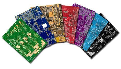
Solder Mask Colors
Solder masks are available in a variety of colors, with green being the most common. Other popular colors include:
- Blue
- Red
- Yellow
- Black
- White
The choice of color is often based on aesthetic preferences, but it can also serve functional purposes. For example, white solder masks are sometimes used to improve the visibility of component markings and labels.
Solder Mask Design Considerations
When designing a PCB with a solder mask, several factors should be taken into account:
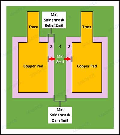
1. Solder Mask Clearance
The solder mask should be designed with appropriate clearances around pads and other exposed copper features. Insufficient clearance can lead to problems during soldering, such as solder mask contamination or difficulty in achieving proper solder joints.
2. Solder Mask Expansion
During the curing process, the solder mask may expand slightly. This expansion should be accounted for in the design to ensure that the final dimensions of the solder mask openings are within specification.
3. Solder Mask Thickness
The thickness of the solder mask can affect its insulation properties and durability. Typical solder mask thicknesses range from 0.5 to 2 mils (0.0127 to 0.0508 mm).
4. Solder Mask Compatibility
The solder mask material should be compatible with the PCB substrate, copper plating, and any other materials used in the manufacturing process. Incompatible materials can lead to adhesion problems or other defects.
Advantages of Using a PCB Solder Mask
Using a solder mask on a PCB offers several advantages:
- Improved reliability: The solder mask protects the copper traces from oxidation and other environmental factors, improving the long-term reliability of the PCB.
- Better electrical insulation: The solder mask provides a layer of insulation between the copper traces, reducing the risk of short circuits and other electrical issues.
- Enhanced manufacturability: The solder mask helps to prevent solder bridges from forming between closely spaced pads, making the soldering process more reliable and efficient.
- Increased durability: The solder mask provides a protective layer that can help to prevent physical damage to the PCB during handling and assembly.
Common Solder Mask Defects and Their Causes
Despite the benefits of using a solder mask, several defects can occur during the manufacturing process:
1. Pinholes
Pinholes are small holes or voids in the solder mask that expose the underlying copper. They can be caused by:
– Contamination on the PCB surface before solder mask application
– Improper cleaning or surface preparation
– Bubbles or voids in the solder mask material
2. Solder Mask Peeling
Solder mask peeling occurs when the mask separates from the PCB surface. Causes include:
– Poor adhesion between the solder mask and the PCB surface
– Incompatible materials
– Excessive stress during thermal cycling
3. Solder Mask Discoloration
Discoloration of the solder mask can occur due to:
– Exposure to high temperatures during soldering or other processes
– Chemical reactions with flux or other materials
– UV exposure over time
4. Solder Mask Misregistration
Misregistration occurs when the solder mask openings are not aligned properly with the pads or other features on the PCB. This can be caused by:
– Incorrect artwork or film alignment during exposure
– Stretching or distortion of the solder mask material during application
– Improper handling or storage of the PCB
| Defect | Causes |
|---|---|
| Pinholes | Contamination, improper cleaning, bubbles/voids |
| Peeling | Poor adhesion, incompatible materials, excessive stress |
| Discoloration | High temperatures, chemical reactions, UV exposure |
| Misregistration | Incorrect artwork/film alignment, material distortion, improper handling |
Frequently Asked Questions (FAQ)
1. What is the difference between a solder mask and a conformal coating?
A solder mask is applied to the PCB before the soldering process and is primarily used to protect the copper traces and prevent solder bridges. A conformal coating is applied after the components have been soldered to the PCB and provides additional protection against moisture, dust, and other environmental factors.
2. Can a PCB be manufactured without a solder mask?
Yes, PCBs can be manufactured without a solder mask. However, this is not recommended for most applications, as the exposed copper traces are more susceptible to oxidation, short circuits, and physical damage.
3. How does the color of the solder mask affect the performance of the PCB?
The color of the solder mask does not directly affect the electrical performance of the PCB. However, some colors may be more susceptible to UV degradation over time, which can impact the long-term reliability of the PCB.
4. Can a damaged solder mask be repaired?
In most cases, a damaged solder mask cannot be easily repaired. If the damage is localized and does not affect the electrical functionality of the PCB, it may be possible to apply a small amount of solder mask material to the affected area. However, if the damage is extensive or compromises the electrical integrity of the PCB, the board may need to be scrapped and replaced.
5. What is the typical thickness of a solder mask?
The typical thickness of a solder mask ranges from 0.5 to 2 mils (0.0127 to 0.0508 mm). The exact thickness will depend on the specific requirements of the PCB, such as the desired level of insulation and protection.
In conclusion, a PCB solder mask is an essential component in the manufacturing of reliable and high-quality printed circuit boards. By understanding the types, application processes, design considerations, and potential defects associated with solder masks, PCB designers and manufacturers can ensure that their boards meet the necessary performance and reliability standards. As PCB technology continues to evolve, the importance of effective solder masking will only continue to grow, making it a critical aspect of modern electronics manufacturing.
No responses yet