Introduction to PCB Slots
PCB slots are an essential component in many printed circuit board (PCB) designs. They serve various purposes, such as providing mechanical support, allowing for the insertion of connectors or modules, and facilitating the mounting of components. In this comprehensive article, we will explore the details of PCB slots, their types, design considerations, and best practices for incorporating them into your YRAYPCB design.
Types of PCB Slots
Edge Slots
Edge slots are commonly used in PCB designs to accommodate connectors or provide a means for inserting the board into a chassis or enclosure. These slots are typically located along the edges of the PCB and can have various shapes and sizes depending on the specific requirements of the design.
Mounting Slots
Mounting slots are used to secure the PCB to a chassis or enclosure using screws or other fasteners. These slots are strategically placed on the board to ensure proper alignment and stability. The size and shape of the mounting slots depend on the type of fasteners being used and the mechanical requirements of the design.
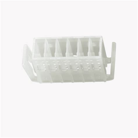
Component Slots
Component slots are used to accommodate through-hole components or provide additional mechanical support for surface-mount components. These slots are designed to match the size and shape of the component leads or pins, allowing for easy insertion and soldering.
Ventilation Slots
Ventilation slots are incorporated into PCB designs to improve air flow and heat dissipation. These slots are particularly important in designs with high-power components or in applications where thermal management is critical. The size, shape, and placement of ventilation slots depend on the specific cooling requirements of the design.

Design Considerations for PCB Slots
Mechanical Stability
When designing PCB slots, it is crucial to consider the mechanical stability of the board. The slots should be placed in a way that minimizes stress and strain on the PCB, particularly in areas where connectors or heavy components are located. Proper placement and sizing of the slots can help prevent warping, cracking, or other mechanical failures.
Electrical Clearance
PCB slots should be designed with sufficient electrical clearance to avoid short circuits or unintended electrical connections. The clearance requirements depend on the voltage levels and the spacing between adjacent traces or components. It is important to follow the design guidelines and standards specific to your application to ensure proper electrical clearance.
Manufacturing Constraints
The manufacturing process imposes certain constraints on the design of PCB slots. The minimum slot width and the spacing between slots are determined by the capabilities of the manufacturing equipment and the tolerances of the fabrication process. It is essential to consult with your PCB manufacturer and adhere to their design guidelines to ensure the slots can be accurately and reliably produced.
Assembly Considerations
PCB slots should be designed with the assembly process in mind. The slots should provide adequate space for the insertion of connectors or components and allow for easy access during soldering or inspection. Additionally, the placement of the slots should consider the orientation and alignment of the board during the assembly process to avoid any conflicts or challenges.

Best Practices for PCB Slot Design
Use Standard Slot Sizes
Whenever possible, use standard slot sizes that are commonly available and compatible with existing connectors or components. This approach simplifies the design process, reduces manufacturing costs, and ensures better compatibility with off-the-shelf components.
Provide Adequate Clearance
Ensure that there is sufficient clearance around the slots to accommodate any tolerances in the manufacturing process and to prevent interference with adjacent components or features. The clearance requirements may vary depending on the specific design and the capabilities of the manufacturing process.
Reinforce Critical Areas
In areas where mechanical stress is expected, such as around connectors or mounting points, consider reinforcing the slots with additional material or by using plated through-holes. This reinforcement helps distribute the stress and prevents cracking or damage to the PCB.
Optimize Slot Placement
Carefully plan the placement of slots to optimize the overall layout of the PCB. Consider the routing of traces, the placement of components, and the mechanical requirements of the design. Strive for a balanced and symmetrical placement of slots to minimize stress and improve the overall stability of the board.
Collaborate with Manufacturers
Work closely with your PCB manufacturer throughout the design process. Seek their expertise and guidance on slot design, manufacturing constraints, and best practices. They can provide valuable insights and help you optimize your design for manufacturability and reliability.

PCB Slot Design Tools and Software
To facilitate the design of PCB slots, various software tools and platforms are available. These tools offer features and capabilities specifically tailored for slot design, such as:
- Automated slot creation and placement
- Design rule checks for slot dimensions and clearances
- 3D modeling and visualization of slots
- Integration with PCB layout and routing tools
Some popular PCB design software that support slot design include:
| Software | Manufacturer | Key Features |
|---|---|---|
| Altium Designer | Altium | Comprehensive slot design tools, 3D modeling |
| Eagle | Autodesk | User-friendly interface, extensive libraries |
| KiCad | KiCad EDA | Open-source, community-driven development |
| OrCAD | Cadence | Powerful constraint management, simulation |
When selecting a PCB design software, consider factors such as ease of use, compatibility with your existing design workflow, and the specific requirements of your project.
Frequently Asked Questions (FAQ)
-
What are the minimum slot dimensions for a standard PCB?
The minimum slot dimensions depend on the capabilities of your PCB manufacturer and the specific requirements of your design. Typically, the minimum slot width is around 0.5mm to 1mm, but it is always best to consult with your manufacturer for their specific guidelines. -
How do I determine the appropriate clearance for PCB slots?
The appropriate clearance for PCB slots depends on several factors, including the voltage levels, the spacing between adjacent traces or components, and the manufacturing tolerances. Refer to the design guidelines and standards specific to your application, such as the IPC standards, to determine the proper clearance requirements. -
Can I use PCB slots for high-current applications?
Yes, PCB slots can be used in high-current applications, but special considerations must be taken. Ensure that the slots are properly sized and reinforced to handle the expected current levels and minimize resistance. Additionally, consider the thermal management aspects and provide adequate cooling mechanisms to dissipate heat generated by high-current components. -
How can I prevent cracking or damage around PCB slots?
To prevent cracking or damage around PCB slots, follow these best practices: - Provide adequate clearance and spacing around the slots
- Reinforce critical areas with additional material or plated through-holes
- Optimize slot placement to minimize stress and ensure mechanical stability
-
Adhere to the manufacturing guidelines and tolerances provided by your PCB manufacturer
-
Are there any specific considerations for designing slots in flexible PCBs?
When designing slots in flexible PCBs, consider the flexibility and bending requirements of the application. Ensure that the slots do not compromise the structural integrity of the flexible substrate and provide adequate strain relief to prevent damage during flexing. Additionally, consider the placement of the slots relative to the bending axes to minimize stress and ensure reliable performance.
Conclusion
PCB slots play a crucial role in the design and functionality of printed circuit boards. By understanding the different types of slots, their design considerations, and best practices, you can effectively incorporate slots into your YRAYPCB design. Remember to consider factors such as mechanical stability, electrical clearance, manufacturing constraints, and assembly requirements when designing PCB slots.
Collaborate closely with your PCB manufacturer and leverage the available design tools and software to streamline the slot design process and ensure the best possible outcome for your project. By following the guidelines and best practices outlined in this article, you can create robust and reliable PCB designs that meet your specific requirements.
No responses yet