Introduction to PCB Design Guidelines
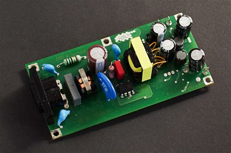
Printed Circuit Boards (PCBs) are the backbone of modern electronics. They provide a platform for mounting and interconnecting electronic components, ensuring proper functionality and reliability. When designing a PCB, it is crucial to follow certain guidelines to ensure optimal performance, manufacturability, and cost-effectiveness. In this article, we will discuss the essential guidelines for PCB size and pad size, helping you create robust and efficient designs.
Understanding PCB Sizes
Standard PCB Sizes
PCBs come in various sizes, depending on the application and the available space within the device. Some common standard PCB sizes include:
| PCB Size | Dimensions (mm) | Typical Applications |
|---|---|---|
| Small | 25 x 25 | Wearables, IoT devices |
| Medium | 50 x 50 | Smartphones, tablets |
| Large | 100 x 100 | Laptops, desktops |
| Extra Large | 200 x 200 | Industrial control systems |
It’s important to choose the appropriate PCB size based on your specific requirements, considering factors such as component placement, routing, and mechanical constraints.
Custom PCB Sizes
In some cases, standard PCB sizes may not suit your project’s needs. Custom PCB sizes offer flexibility in designing boards that fit unique form factors or accommodate specific component layouts. When opting for a custom PCB size, keep in mind the following considerations:
- Manufacturing capabilities of your chosen PCB fabricator
- Minimum and maximum board dimensions supported
- Aspect ratio limitations
- Panelization options for cost-effective production

PCB Thickness Guidelines
The thickness of a PCB plays a crucial role in its mechanical strength, thermal management, and signal integrity. Common PCB thicknesses include:
| Thickness (mm) | Copper Weight (oz) | Application |
|---|---|---|
| 0.8 | 1 | Simple, low-cost designs |
| 1.6 | 1 or 2 | General-purpose, double-sided boards |
| 2.4 | 2 or 3 | Complex, multilayer boards |
| 3.2 | 3 or 4 | High-power, heavy copper designs |
Consider the following factors when selecting the appropriate PCB thickness:
- Number of layers required
- Copper weight for current carrying capacity
- Mechanical strength and rigidity requirements
- Thermal dissipation needs

Pad Size Guidelines
Pads are the copper areas on a PCB where components are soldered. Proper pad sizing is essential for reliable soldering, component placement, and manufacturability. Consider the following guidelines when designing pads:
Pad-to-Hole Ratio
The pad-to-hole ratio is the relationship between the pad diameter and the hole diameter. A typical pad-to-hole ratio is 1.8:1, meaning the pad diameter is 1.8 times larger than the hole diameter. This ratio ensures sufficient annular ring for reliable soldering and prevents pad lifting or detachment.
Pad Shape and Size
Pads can be circular, oval, or rectangular, depending on the component type and soldering requirements. Common pad sizes for various component packages include:
| Component Package | Pad Size (mm) |
|---|---|
| 0402 | 0.5 x 0.5 |
| 0603 | 0.8 x 0.8 |
| 0805 | 1.0 x 1.2 |
| SOIC-8 | 2.0 x 0.6 |
| TQFP-44 | 0.8 x 0.4 |
When determining pad sizes, consider the following factors:
- Component dimensions and tolerances
- Soldering process (e.g., reflow, wave, hand soldering)
- Clearance requirements between adjacent pads
- Assembly and rework considerations
Solder Mask Openings
Solder mask is a protective layer applied over the copper traces on a PCB, leaving only the pads exposed for soldering. The solder mask opening (SMO) is the area around the pad where the solder mask is removed. Proper SMO design ensures accurate solder joint formation and prevents solder bridging. Consider the following guidelines for SMO design:
- SMO should be larger than the pad size by 0.05 to 0.1 mm on each side
- Maintain a minimum solder mask web between adjacent pads to prevent shorts
- Use teardrops or chamfered corners to prevent solder mask slivers
Routing and Clearance Guidelines
Proper routing and clearance guidelines ensure signal integrity, manufacturability, and reliability of the PCB. Consider the following guidelines:
Trace Width and Spacing
Trace width and spacing determine the current carrying capacity and the minimum clearance between adjacent traces. Use the following guidelines:
| Trace Current | Trace Width (mm) | Trace Spacing (mm) |
|---|---|---|
| < 0.5 A | 0.2 – 0.3 | 0.2 |
| 0.5 – 1 A | 0.3 – 0.4 | 0.25 |
| 1 – 2 A | 0.4 – 0.6 | 0.3 |
| > 2 A | > 0.6 | > 0.3 |
- Increase trace width for high-current paths
- Maintain adequate spacing to prevent crosstalk and signal interference
- Follow the PCB manufacturer’s design rules for minimum trace width and spacing
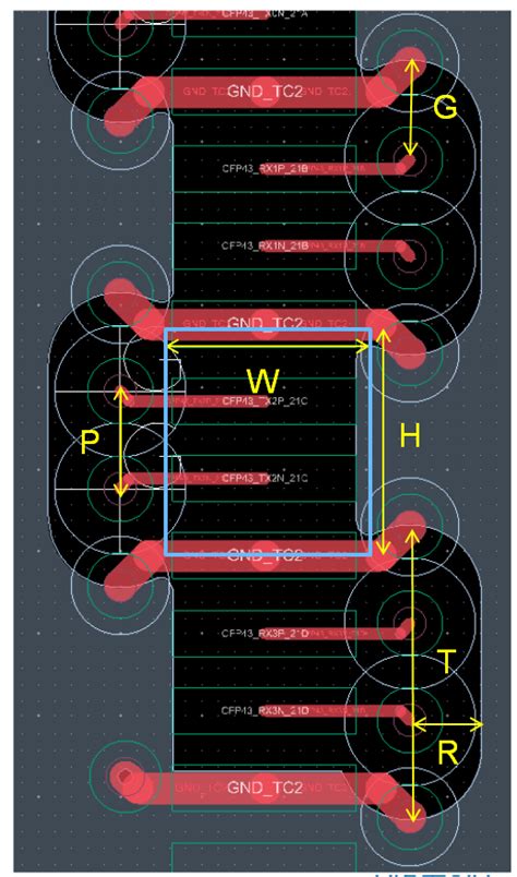
Via Size and Placement
Vias are used to connect traces on different layers of a PCB. Consider the following guidelines for via design:
- Use appropriate via sizes based on the hole diameter and the PCB thickness
- Place vias at least one pad diameter away from component pads
- Avoid placing vias under components to prevent assembly issues
- Use via tenting or filling for improved reliability and manufacturability
Component Placement Guidelines
Proper component placement is crucial for optimal PCB performance and manufacturability. Consider the following guidelines:
- Place components in a logical and organized manner, grouping related components together
- Orient components for easy assembly and soldering
- Maintain sufficient clearance between components for thermal management and rework access
- Consider the component height and the available space within the enclosure
- Place sensitive components away from potential sources of interference
Manufacturing Considerations
When designing a PCB, it’s important to consider the manufacturing process to ensure cost-effectiveness and reliability. Consider the following manufacturing guidelines:
- Choose a reputable PCB manufacturer with proven capabilities
- Provide clear and accurate manufacturing files, including Gerber files and drill files
- Specify the required PCB finish (e.g., HASL, ENIG, OSP) based on the application and the component requirements
- Consider panelization for efficient production and cost savings
- Communicate any special requirements or constraints to the manufacturer upfront
Frequently Asked Questions (FAQ)
1. What is the minimum PCB size that can be manufactured?
The minimum PCB size depends on the capabilities of the PCB manufacturer. Typically, PCB manufacturers can produce boards as small as 25 x 25 mm. However, it’s always best to consult with your chosen manufacturer to determine their specific capabilities and limitations.
2. How do I choose the appropriate PCB thickness for my design?
The choice of PCB thickness depends on several factors, including the number of layers required, the copper weight for current carrying capacity, mechanical strength and rigidity requirements, and thermal dissipation needs. Generally, 1.6 mm thickness is suitable for most general-purpose, double-sided boards, while thicker boards (2.4 mm or 3.2 mm) are used for complex, multilayer designs or high-power applications.
3. What is the recommended pad-to-hole ratio for reliable soldering?
A typical pad-to-hole ratio is 1.8:1, meaning the pad diameter is 1.8 times larger than the hole diameter. This ratio ensures sufficient annular ring for reliable soldering and prevents pad lifting or detachment. However, the exact ratio may vary depending on the specific component and soldering requirements.
4. How can I ensure proper clearance between traces to prevent signal interference?
To prevent signal interference and crosstalk, maintain adequate spacing between traces. The specific spacing requirements depend on the trace current and the PCB manufacturer’s design rules. As a general guideline, maintain a minimum spacing of 0.2 mm for low-current traces (< 0.5 A) and increase the spacing for higher-current traces. It’s important to consult with your PCB manufacturer and follow their specific design rules for trace spacing.
5. What are some best practices for component placement on a PCB?
When placing components on a PCB, consider the following best practices:
- Place components in a logical and organized manner, grouping related components together for easier routing and signal integrity.
- Orient components for easy assembly and soldering, ensuring that the component markings are visible and the leads are accessible.
- Maintain sufficient clearance between components for thermal management and rework access. Consider the component height and the available space within the enclosure.
- Place sensitive components, such as high-speed devices or analog circuits, away from potential sources of interference, such as power supplies or digital circuits.
- Follow the component manufacturer’s recommended land pattern and placement guidelines for optimal performance and reliability.
By following these component placement best practices, you can improve the manufacturability, reliability, and performance of your PCB design.
Conclusion
Designing a PCB requires careful consideration of various guidelines and best practices to ensure optimal performance, manufacturability, and cost-effectiveness. By understanding and following the guidelines for PCB size, pad size, routing, clearance, and component placement, you can create robust and reliable PCB designs.
Remember to collaborate closely with your PCB manufacturer, providing clear and accurate manufacturing files and communicating any special requirements or constraints upfront. By working together and adhering to industry standards and best practices, you can bring your PCB design from concept to reality with confidence.
No responses yet