What are PCB Shields?
PCB shields, also known as electromagnetic interference (EMI) shields or radio frequency interference (RFI) shields, are protective enclosures designed to reduce the electromagnetic interference that can affect the performance of electronic devices. These shields are typically made of conductive materials, such as metal or metalized plastic, and are placed over sensitive electronic components on a printed circuit board (PCB).
Types of PCB Shields
There are several types of PCB shields available, each designed to address specific shielding requirements:
-
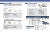
One-piece shields: These shields are made from a single piece of metal, usually stamped or formed to fit over the components on a PCB. They are cost-effective and easy to install but may not provide as much protection as multi-piece shields.
-
Two-piece shields: Consisting of a frame and a removable cover, two-piece shields offer better protection than one-piece shields. They allow for easier access to the components for maintenance or debugging purposes.
-
Custom shields: For unique shielding requirements, custom shields can be designed and manufactured to fit specific PCB layouts and components.
Materials Used in PCB Shields
PCB shields are typically made from conductive materials that effectively block electromagnetic interference. Some common materials include:
-
Aluminum: Lightweight, cost-effective, and easy to work with, aluminum is a popular choice for PCB shields.
-
Stainless steel: Offers excellent shielding performance and corrosion resistance but is more expensive and difficult to work with compared to aluminum.
-
Copper: Provides superior shielding effectiveness but is more costly than aluminum and stainless steel.
-
Metalized plastic: A plastic substrate coated with a conductive material, such as nickel or copper, offers good shielding performance and is lighter than metal shields.
Why are PCB Shields Important?
PCB shields play a crucial role in ensuring the proper functioning and reliability of electronic devices. They offer several key benefits:
1. Reducing Electromagnetic Interference (EMI)
EMI can cause various issues in electronic devices, such as signal degradation, data corruption, and system malfunctions. By enclosing sensitive components within a conductive shield, PCB shields help to minimize the impact of EMI on the device’s performance.
2. Preventing Radio Frequency Interference (RFI)
RFI, a subset of EMI, specifically refers to interference caused by radio frequency signals. PCB shields help to block RFI from entering or escaping the shielded area, reducing the likelihood of interference with other electronic devices or wireless communication systems.
3. Enhancing Signal Integrity
By reducing EMI and RFI, PCB shields help to maintain the integrity of the signals within the shielded area. This is particularly important for high-speed digital circuits and sensitive analog circuits, where even minor interference can lead to signal degradation and system errors.
4. Meeting Regulatory Requirements
Many countries and regions have strict regulations regarding electromagnetic compatibility (EMC) for electronic devices. PCB shields can help devices meet these requirements by reducing the electromagnetic emissions generated by the device and improving its immunity to external interference.

Designing PCB Shields
When designing PCB shields, several factors must be considered to ensure optimal shielding performance:
1. Shielding Effectiveness
The shielding effectiveness (SE) of a PCB shield is a measure of its ability to attenuate electromagnetic energy. SE is typically expressed in decibels (dB) and is a function of the shield’s material, thickness, and aperture size. Higher SE values indicate better shielding performance.
2. Aperture Size
Apertures, or openings, in a PCB shield can allow electromagnetic energy to enter or escape the shielded area. To maintain good shielding effectiveness, it is essential to minimize the size and number of apertures in the shield. As a general rule, apertures should be kept as small as possible, typically less than 1/20th of the wavelength of the highest frequency of concern.
3. Grounding
Proper grounding is crucial for the effective performance of PCB shields. The shield should be electrically connected to the PCB’s ground plane through low-impedance paths, such as conductive gaskets or multiple ground points. This helps to prevent the shield from becoming an antenna and radiating electromagnetic energy.
4. Material Selection
The choice of shielding material depends on factors such as shielding effectiveness requirements, weight, cost, and environmental conditions. Aluminum is a common choice for its low cost and ease of fabrication, while stainless steel and copper offer better shielding performance but at a higher cost.
5. Mechanical Design
PCB shields must be designed to fit securely over the components they are intended to protect, without interfering with other components or connectors on the PCB. The shield design should also consider the assembly process, ensuring that the shield can be easily installed and removed for maintenance or debugging purposes.

Installing and Testing PCB Shields
Proper installation and testing of PCB shields are essential to ensure their effectiveness in reducing electromagnetic interference.
Installation Techniques
There are several methods for installing PCB shields, depending on the shield type and PCB design:
-
Soldering: One-piece shields and the frames of two-piece shields can be soldered directly to the PCB’s ground plane. This provides a secure, low-impedance connection between the shield and the ground.
-
Snap-on: Some shields are designed with snap-on features that allow them to be easily attached to the PCB without soldering. This method is often used for two-piece shields, where the cover can be snapped onto the frame.
-
Conductive adhesives: For situations where soldering is not practical, conductive adhesives can be used to attach the shield to the PCB. These adhesives provide an electrical connection between the shield and the ground plane while mechanically securing the shield in place.
Testing PCB Shields
After installation, it is important to test the effectiveness of the PCB shield in reducing electromagnetic interference. There are several methods for testing shield performance:
-
EMI scanning: An EMI scanner can be used to measure the electromagnetic emissions from the shielded device. By comparing the emissions with and without the shield in place, the shielding effectiveness can be determined.
-
Near-field probing: A near-field probe can be used to measure the electromagnetic fields in close proximity to the shielded components. This method can help identify any leaks or weak points in the shield.
-
Transfer impedance measurement: The transfer impedance of a shield is a measure of its ability to attenuate electromagnetic energy. By measuring the transfer impedance, the shielding effectiveness can be quantified.

Common Challenges and Solutions in PCB shielding
While PCB shields are an effective tool for reducing electromagnetic interference, there are several challenges that designers and engineers may face when implementing them.
1. Inadequate Shielding Effectiveness
If a PCB shield fails to provide sufficient shielding effectiveness, it may be due to several factors, such as improper material selection, inadequate thickness, or excessive aperture size. To address this issue, consider using a higher-grade shielding material, increasing the shield thickness, or redesigning the shield to minimize apertures.
2. Poor Grounding
Inadequate grounding can compromise the effectiveness of a PCB shield, allowing electromagnetic energy to leak into or out of the shielded area. Ensure that the shield is properly connected to the PCB’s ground plane through low-impedance paths, such as conductive gaskets or multiple ground points. Additionally, make sure that the ground plane itself is well-designed and free of discontinuities.
3. Mechanical Interference
PCB shields can sometimes interfere with other components or connectors on the PCB, leading to assembly or functional issues. To avoid this, carefully design the shield to fit securely over the intended components without impeding other parts of the PCB. Consider using computer-aided design (CAD) tools to create accurate 3D models of the shield and PCB to identify potential interferences.
4. Cost Constraints
Implementing PCB shields can add to the overall cost of a device, particularly if high-performance materials or custom designs are required. To minimize costs, consider using standard shield sizes and shapes when possible, and select materials that offer a good balance of shielding effectiveness and affordability. In some cases, alternative shielding methods, such as conductive coatings or gaskets, may be more cost-effective than traditional PCB shields.
Frequently Asked Questions (FAQ)
-
Q: What is the difference between EMI and RFI?
A: EMI (electromagnetic interference) is a broad term that refers to any electromagnetic disturbance that can disrupt the performance of electronic devices. RFI (radio frequency interference) is a specific type of EMI that occurs in the radio frequency spectrum, typically between 3 kHz and 300 GHz. -
Q: Can PCB shields completely eliminate EMI?
A: While PCB shields can significantly reduce EMI, it is nearly impossible to completely eliminate it. The effectiveness of a shield depends on factors such as material selection, design, and proper installation. In some cases, additional shielding measures, such as filtered connectors or conductive gaskets, may be necessary to achieve the desired level of EMI reduction. -
Q: How do I select the right material for my PCB shield?
A: The choice of shielding material depends on several factors, including shielding effectiveness requirements, weight, cost, and environmental conditions. Aluminum is a popular choice for its low cost and ease of fabrication, while stainless steel and copper offer better shielding performance but at a higher cost. Consider consulting with a shielding expert or manufacturer to determine the best material for your specific application. -
Q: Can I use a PCB shield in a Flexible Circuit Design?
A: Yes, PCB shields can be used in flexible circuit designs, but they may require special considerations. Flexible shields, such as those made from metalized fabric or conductive elastomers, can be used to provide shielding without compromising the flexibility of the circuit. Additionally, the shield design may need to account for the bending and flexing of the circuit to ensure proper fit and function. -
Q: How do I ensure proper grounding of my PCB shield?
A: To ensure proper grounding, the PCB shield should be electrically connected to the PCB’s ground plane through low-impedance paths. This can be achieved through methods such as soldering the shield directly to the ground plane, using conductive gaskets or adhesives, or providing multiple ground points around the shield’s perimeter. It is also important to ensure that the ground plane itself is well-designed and free of discontinuities that could compromise the shielding effectiveness.
Conclusion
PCB shields are an essential component in the design of electronic devices, helping to reduce electromagnetic interference and ensure proper device performance. By understanding the types of shields available, the materials used, and the key design considerations, engineers and designers can effectively implement PCB shields in their projects.
Proper installation and testing are crucial to ensure the effectiveness of PCB shields, and common challenges such as inadequate shielding effectiveness, poor grounding, and mechanical interference must be addressed through careful design and material selection.
As the demand for reliable, high-performance electronic devices continues to grow, the importance of effective PCB shielding will only increase. By staying informed about the latest advances in shielding technology and best practices for design and implementation, engineers and designers can create products that meet the evolving needs of the market while maintaining optimal electromagnetic compatibility.

No responses yet