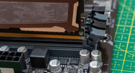
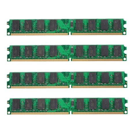
Introduction to DDR4 Memory and PCB Routing
DDR4 (Double Data Rate 4) is the latest generation of memory technology used in modern computing systems. It offers higher performance, lower power consumption, and increased density compared to its predecessors. When designing a PCB (Printed Circuit Board) that incorporates DDR4 memory devices, it is crucial to follow proper routing guidelines to ensure optimal signal integrity and system reliability.
In this article, we will discuss the key considerations and best practices for PCB routing when using DDR4 memory devices. We will cover topics such as signal integrity, power delivery, layout recommendations, and common pitfalls to avoid.
Understanding DDR4 Memory Specifications
Before diving into PCB routing guidelines, it is essential to understand the specifications and characteristics of DDR4 memory devices. DDR4 memory operates at higher frequencies and lower voltages compared to previous generations, which poses new challenges for PCB design.
DDR4 Memory Characteristics
| Parameter | DDR4 Specification |
|---|---|
| Operating Voltage | 1.2 V |
| Data Rate | 1600 MT/s to 3200 MT/s |
| Prefetch | 8n |
| Bank Groups | 4 |
| Banks per Group | 4 |
| Burst Length | BL8 (fixed) |
DDR4 memory devices have tighter timing requirements and more stringent signal integrity constraints. They also introduce new features such as bank groups and command/address parity for improved performance and reliability.
Signal Integrity Considerations
Signal integrity is a critical aspect of PCB routing for DDR4 memory devices. Proper signal routing ensures that data and control signals maintain their integrity and avoid issues such as crosstalk, reflections, and timing violations.
Impedance Matching
Impedance matching is crucial for maintaining signal integrity in DDR4 memory interfaces. The characteristic impedance of the PCB traces should match the impedance of the DDR4 memory devices and the controller. Typically, a 50-ohm impedance is used for single-ended signals, while a 100-ohm differential impedance is used for differential signals.
To achieve proper impedance matching, consider the following guidelines:
– Use controlled impedance PCB stackup with well-defined dielectric materials and thicknesses.
– Adjust trace widths and spacing to achieve the desired characteristic impedance.
– Minimize impedance discontinuities by avoiding abrupt changes in trace geometry.
Length Matching
Length matching is another important consideration for DDR4 memory routing. The data, address, and control signals should have equal lengths to ensure synchronous arrival at the memory devices. Length mismatches can lead to timing violations and degrade system performance.
Follow these guidelines for length matching:
– Route all signals within a byte lane or group to have equal lengths.
– Use serpentine routing techniques to add length to shorter traces and match the longer traces.
– Keep the maximum length difference within a byte lane or group to less than 10 ps.
Crosstalk Mitigation
Crosstalk is a phenomenon where signals from adjacent traces interfere with each other, causing signal integrity issues. In DDR4 memory interfaces, crosstalk can lead to data corruption and timing violations.
To mitigate crosstalk, consider the following techniques:
– Increase the spacing between adjacent traces to reduce coupling.
– Use ground shielding between sensitive signals to provide isolation.
– Avoid long parallel runs of adjacent traces.
– Stagger the routing of adjacent signals to minimize coupling.

Power Delivery Considerations
Proper power delivery is essential for stable and reliable operation of DDR4 memory devices. The power distribution network (PDN) should provide clean and stable power to the memory devices while minimizing noise and voltage variations.
Power Plane Design
Use dedicated power planes for the DDR4 memory power supplies (VDD and VDDQ). The power planes should be placed close to the surface layer to minimize inductance and provide a low-impedance path for the power supply current.
Consider the following guidelines for power plane design:
– Use wide and uninterrupted power planes to minimize voltage drop and inductance.
– Place the power planes close to the memory devices to reduce the current loop area.
– Avoid splitting the power planes or introducing large gaps, as it can increase inductance and degrade power integrity.
Decoupling Capacitors
Decoupling capacitors play a critical role in maintaining power integrity and reducing high-frequency noise in DDR4 memory interfaces. Place decoupling capacitors close to the memory devices to provide a local energy reservoir and filter out power supply noise.
Consider the following guidelines for decoupling capacitor placement:
– Use a combination of bulk and ceramic capacitors to cover different frequency ranges.
– Place the decoupling capacitors as close to the memory devices as possible to minimize the current loop area.
– Use multiple decoupling capacitors in parallel to reduce the effective series inductance (ESL) and improve high-frequency performance.
Power Sequence and Ramp Rates
DDR4 memory devices have specific requirements for power-up and power-down sequences and ramp rates. Violating these requirements can lead to memory initialization failures and stability issues.
Ensure that the power supplies for DDR4 memory devices follow the recommended sequence and ramp rates:
– Power up the VDD supply before the VDDQ supply.
– Maintain the proper ramp rates for VDD and VDDQ supplies as specified in the DDR4 memory datasheet.
– Use power sequencing circuits or voltage supervisors to control the power-up and power-down sequences.
Layout Recommendations
Proper layout is crucial for ensuring signal integrity and power delivery in DDR4 memory interfaces. Follow these layout recommendations to optimize the PCB routing:
Component Placement
- Place the DDR4 memory devices close to the memory controller to minimize trace lengths and signal propagation delays.
- Arrange the memory devices symmetrically to achieve equal trace lengths and simplify routing.
- Keep the decoupling capacitors close to the memory devices to minimize the current loop area.
Trace Routing
- Route the data, address, and control signals on the top or bottom layer to minimize the number of vias.
- Use 45-degree angle turns instead of 90-degree turns to reduce reflections and improve signal integrity.
- Avoid routing traces over gaps or splits in the power planes to minimize impedance discontinuities.
Via Optimization
- Minimize the number of vias in the signal paths to reduce inductance and reflections.
- Use microvias or blind/buried vias when transitioning between layers to reduce the via stub effect.
- Place the vias close to the memory devices to minimize the stub length.
Ground Referencing
- Provide a continuous ground reference plane beneath the DDR4 memory signals to minimize impedance discontinuities and improve signal integrity.
- Use ground stitching vias to connect the ground planes on different layers and provide a low-impedance return path for the signals.
Common Pitfalls and Considerations
When routing PCBs for DDR4 memory devices, be aware of the following common pitfalls and considerations:
Trace Impedance Discontinuities
Avoid abrupt changes in trace geometry, such as width variations or layer transitions, as they can cause impedance discontinuities and reflections. Maintain consistent trace widths and use smooth transitions when necessary.
Crosstalk and Signal Coupling
Minimize crosstalk and signal coupling by providing adequate spacing between traces, using ground shielding, and staggering the routing of adjacent signals. Pay special attention to the routing of clock signals and keep them away from other sensitive signals.
Power Supply Noise
Ensure that the power supplies for DDR4 memory devices are clean and stable. Use proper decoupling techniques, such as placing decoupling capacitors close to the devices and using power planes with low impedance. Avoid routing noisy signals or high-speed signals near the power supplies.
Thermal Management
DDR4 memory devices generate heat during operation, which can affect their performance and reliability. Consider the thermal management aspects of the PCB design, such as providing adequate cooling, using thermal vias to dissipate heat, and avoiding placing heat-generating components near the memory devices.
Signal Integrity Simulation
Perform signal integrity simulations to validate the PCB routing and identify potential issues before fabrication. Use tools like SPICE or specialized PCB design software to simulate the signal behavior and ensure that the routing meets the required specifications.
Frequently Asked Questions (FAQ)
- What is the recommended impedance for DDR4 memory signals?
- For single-ended signals, a 50-ohm impedance is typically used. For differential signals, a 100-ohm differential impedance is recommended.
- How critical is length matching for DDR4 memory signals?
- Length matching is crucial for ensuring synchronous arrival of signals at the memory devices. The maximum length difference within a byte lane or group should be kept below 10 ps to avoid timing violations.
- What are the benefits of using power planes for DDR4 memory power delivery?
- Power planes provide a low-impedance path for the power supply current, minimizing voltage drop and inductance. They also help in reducing power supply noise and improving power integrity.
- Why is it important to place decoupling capacitors close to the DDR4 memory devices?
- Placing decoupling capacitors close to the memory devices minimizes the current loop area and reduces the effective series inductance (ESL). This helps in filtering out high-frequency noise and maintaining stable power delivery.
- What are the recommended power-up and power-down sequences for DDR4 memory devices?
- DDR4 memory devices have specific requirements for power-up and power-down sequences. Typically, the VDD supply should be powered up before the VDDQ supply. It is important to follow the recommended sequences and ramp rates specified in the DDR4 memory datasheet to ensure proper initialization and stability.
Conclusion
PCB routing for DDR4 memory devices requires careful consideration of signal integrity, power delivery, and layout techniques. By following the guidelines discussed in this article, such as impedance matching, length matching, crosstalk mitigation, power plane design, and proper component placement, designers can ensure optimal performance and reliability of DDR4 memory interfaces.
It is essential to understand the specifications and requirements of DDR4 memory devices and adhere to the recommended practices during PCB routing. Performing signal integrity simulations and validating the design before fabrication can help identify and resolve potential issues early in the development process.
By paying attention to the common pitfalls and considerations, such as trace impedance discontinuities, crosstalk, power supply noise, and thermal management, designers can minimize the risk of signal integrity problems and ensure the robustness of the DDR4 memory interface.
Proper PCB routing is crucial for achieving the high performance and reliability expected from DDR4 memory devices. By following the guidelines outlined in this article, designers can navigate the complexities of DDR4 memory routing and create successful PCB designs that meet the demanding requirements of modern computing systems.
No responses yet