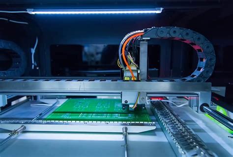
Factors Affecting PCB Manufacturing Cost
Several factors play a crucial role in determining the total cost of PCB manufacturing. These include:
- PCB Design Complexity
- PCB Size and Thickness
- Number of Layers
- Material Selection
- Surface Finish
- Quantity and Economies of Scale
- Lead Time and Turnaround Time
- Additional Services and Features
Let’s explore each of these factors in more detail.
PCB Design Complexity
The complexity of your PCB design has a direct impact on the manufacturing cost. A more intricate design with fine pitch components, high density interconnects (HDI), or advanced features like blind and buried vias will require specialized equipment and expertise, resulting in higher costs. On the other hand, a simpler design with standard components and larger trace widths will be more cost-effective to manufacture.
To optimize your PCB design for cost savings:
- Avoid unnecessary complexity and keep your design as simple as possible while meeting your functional requirements.
- Use standard component packages and avoid fine pitch components when feasible.
- Minimize the use of advanced features like HDI or blind/buried vias unless absolutely necessary.
- Follow the manufacturer’s design guidelines to ensure compatibility with their processes.
PCB Size and Thickness
The size and thickness of your PCB also play a significant role in determining the manufacturing cost. Larger PCBs require more material and may need specialized handling, resulting in higher costs. Similarly, thicker PCBs (e.g., over 1.6mm) may require additional processing steps and longer manufacturing times.
To optimize your PCB size and thickness for cost savings:
- Design your PCB to be as compact as possible while maintaining adequate spacing and clearance.
- Consider using smaller component packages to reduce the overall PCB size.
- Stick to standard PCB thicknesses (e.g., 1.6mm) unless your application demands otherwise.
- Discuss your requirements with your manufacturer to determine the most cost-effective size and thickness options.
Number of Layers
The number of layers in your PCB directly impacts the manufacturing cost. Each additional layer requires more material, processing steps, and time, leading to higher costs. However, using multiple layers can also help you achieve a more compact design and improve signal integrity.
To optimize the number of layers for cost savings:
- Use the minimum number of layers required to meet your design requirements.
- Consider using a 4-layer PCB instead of a 6-layer or 8-layer board when possible.
- Discuss your design with your manufacturer to determine the most cost-effective layer configuration.
| Number of Layers | Relative Cost |
|---|---|
| 1 | 1.0 |
| 2 | 1.5 |
| 4 | 2.0 |
| 6 | 2.8 |
| 8 | 3.5 |
Note: Relative costs are approximate and may vary depending on the manufacturer and other factors.
Material Selection
The choice of PCB material can significantly impact the manufacturing cost. The most common PCB materials are FR-4, which is a cost-effective and versatile option suitable for most applications. However, specialized materials like high-frequency laminates (e.g., Rogers) or metal core PCBs (MCPCBs) can be more expensive due to their unique properties and processing requirements.
To optimize your material selection for cost savings:
- Use FR-4 material when possible, as it is the most cost-effective option for general-purpose PCBs.
- Consider using specialized materials only when your application demands specific properties (e.g., high-frequency performance or thermal management).
- Discuss your material requirements with your manufacturer to identify the most cost-effective options that meet your needs.
Surface Finish
The surface finish applied to your PCB’s exposed copper areas can also affect the manufacturing cost. Some common surface finishes include Hot Air Solder Leveling (HASL), Electroless Nickel Immersion Gold (ENIG), and Immersion Silver (IAg). Each surface finish has its own advantages and cost implications.
To optimize your surface finish selection for cost savings:
- Use HASL when possible, as it is the most cost-effective option for general-purpose PCBs.
- Consider using ENIG or IAg only when your application requires better solderability, flatness, or durability.
- Discuss your surface finish requirements with your manufacturer to determine the most cost-effective option that meets your needs.
| Surface Finish | Relative Cost |
|---|---|
| HASL | 1.0 |
| ENIG | 1.5 |
| IAg | 1.3 |
Note: Relative costs are approximate and may vary depending on the manufacturer and other factors.
Quantity and Economies of Scale
The quantity of PCBs you order has a significant impact on the unit cost. Manufacturers often offer economies of scale, meaning that the unit cost decreases as the order quantity increases. This is because the fixed costs associated with setting up the production process are spread across a larger number of units.
To optimize your order quantity for cost savings:
- Order the maximum quantity that you can afford and reasonably use within your project timeline.
- Consider future demand and plan your orders accordingly to take advantage of volume discounts.
- Discuss your quantity requirements with your manufacturer to determine the most cost-effective order size.
| Quantity | Relative Unit Cost |
|---|---|
| 1-10 | 1.0 |
| 11-50 | 0.8 |
| 51-100 | 0.6 |
| 101-500 | 0.4 |
| 500+ | 0.3 |
Note: Relative unit costs are approximate and may vary depending on the manufacturer and other factors.
Lead Time and Turnaround Time
The lead time and turnaround time for your PCB order can also impact the manufacturing cost. Faster turnaround times often come with a price premium, as manufacturers need to prioritize your order and allocate resources accordingly. On the other hand, longer lead times may offer cost savings but require better planning and project management.
To optimize your lead time and turnaround time for cost savings:
- Plan your project timeline carefully and allow for adequate lead time whenever possible.
- Consider standard lead times (e.g., 5-7 business days) for most orders, as they offer a good balance between cost and speed.
- Discuss your lead time requirements with your manufacturer and explore options that align with your budget and project timeline.
Additional Services and Features
PCB manufacturers often offer additional services and features that can impact the overall cost. These may include:
- PCB Assembly (PCBA)
- Design for Manufacturing (DFM) analysis
- Electrical testing
- Impedance control
- Controlled impedance
- Solder mask color options
- Silkscreen color options
To optimize your use of additional services and features for cost savings:
- Only request additional services and features that are essential to your project’s success.
- Consider performing some tasks in-house (e.g., PCB assembly) if you have the capability and it is cost-effective.
- Discuss your requirements with your manufacturer to identify the most cost-effective options that meet your needs.
Strategies for Maximizing Cost Savings
In addition to optimizing the individual factors discussed above, there are several strategies you can employ to maximize your cost savings in PCB manufacturing:
-
Early Collaboration with Your Manufacturer: Engage with your PCB manufacturer early in the design process to discuss your requirements, constraints, and cost-saving opportunities. Their expertise can help you make informed decisions that optimize your design for manufacturability and cost-effectiveness.
-
Design for Manufacturing (DFM) Analysis: Request a DFM analysis from your manufacturer to identify potential design issues that could increase manufacturing costs or lead to production delays. Addressing these issues early can help you avoid costly redesigns and optimize your PCB for cost savings.
-
Panelization: Consider panelizing your PCBs, which involves placing multiple PCBs on a single panel for production. This can help reduce manufacturing costs by optimizing material usage and minimizing handling time. Discuss panelization options with your manufacturer to determine the most cost-effective approach.
-
Standardization: Where possible, standardize your PCB designs across multiple projects or products. This can help you achieve economies of scale, reduce setup costs, and optimize your inventory management. Standardization also allows you to leverage your manufacturer’s expertise and processes more effectively.
-
Continuous Improvement: Regularly review your PCB designs and manufacturing processes to identify opportunities for cost savings. Stay updated on the latest industry trends, materials, and manufacturing techniques that could help you optimize your costs without compromising quality.

Frequently Asked Questions (FAQ)
-
Q: How can I estimate the cost of my PCB before placing an order?
A: Most PCB manufacturers offer online quotation tools that allow you to input your PCB specifications and receive an instant quote. You can also contact the manufacturer directly with your requirements to obtain a more accurate cost estimate. -
Q: What is the minimum order quantity (MOQ) for PCBs?
A: The MOQ varies depending on the manufacturer and the complexity of your PCB design. Some manufacturers offer low MOQs (e.g., 5-10 pieces) for prototyping and small-scale production, while others may require higher quantities for cost-effective manufacturing. -
Q: How can I balance cost savings with PCB Quality and reliability?
A: To balance cost savings with quality and reliability, focus on optimizing your PCB design for manufacturability, selecting appropriate materials and surface finishes, and collaborating closely with your manufacturer. Avoid compromising on essential features or quality standards that could impact your product’s performance or longevity. -
Q: What are the typical lead times for PCB manufacturing?
A: Lead times vary depending on the manufacturer, the complexity of your PCB design, and the quantity ordered. Standard lead times range from 5-7 business days for simple designs to 2-3 weeks for more complex boards. Expedited options may be available for an additional cost. -
Q: How can I ensure the manufacturability of my PCB design?
A: To ensure the manufacturability of your PCB design, follow industry-standard design guidelines, use appropriate design tools and software, and collaborate closely with your manufacturer. Request a Design for Manufacturing (DFM) analysis to identify and address potential design issues early in the process.

Conclusion
Understanding the various factors that contribute to PCB manufacturing costs is essential for maximizing your cost savings and ensuring the success of your projects. By optimizing your PCB design, selecting appropriate materials and features, and collaborating closely with your manufacturer, you can effectively balance cost, quality, and reliability.
Remember to consider the long-term implications of your design and manufacturing decisions, as well as the total cost of ownership for your products. By taking a strategic approach to PCB manufacturing cost optimization, you can drive innovation, improve profitability, and deliver high-quality products to your customers.

No responses yet