Introduction to PCB Layout
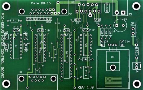
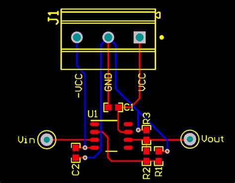
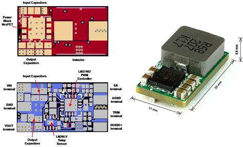
Printed Circuit Board (PCB) layout is a crucial step in the design and manufacture of electronic devices. It involves arranging and connecting electronic components on a board to create a functional circuit. PCB layout software is a specialized tool that helps designers create accurate and efficient PCB designs. In this comprehensive guide, we will explore the various aspects of PCB layout software, including its features, benefits, and popular options available in the market.
What is PCB Layout Software?
PCB layout software is a computer-aided design (CAD) tool used to create PCB designs. It allows designers to place components, route traces, and define the overall layout of the PCB. The software provides a graphical user interface (GUI) where designers can visually arrange the components and connections on the board. It also includes various tools and features to optimize the design, such as auto-routing, design rule checking (DRC), and 3D visualization.

Benefits of Using PCB Layout Software
Using PCB layout software offers several benefits over manual PCB design methods. Some of the key advantages include:
- Increased Efficiency: PCB layout software automates many tedious and time-consuming tasks, such as component placement and trace routing. This significantly reduces the design time and allows designers to focus on more critical aspects of the design.
- Improved Accuracy: PCB layout software ensures precise component placement and trace routing, minimizing the risk of errors. It also includes design rule checking (DRC) features that validate the design against predefined rules, catching potential issues before the board is manufactured.
- Enhanced Collaboration: Many PCB layout software tools support collaborative design, allowing multiple designers to work on the same project simultaneously. This enables better communication and coordination among team members, leading to faster design iterations and improved overall quality.
- 3D Visualization: Advanced PCB layout software provides 3D visualization capabilities, allowing designers to view the PCB design from different angles and identify potential mechanical interference or clearance issues.
- Simplified Revisions: With PCB layout software, making design revisions is much easier compared to manual methods. Designers can quickly modify the layout, update component placement, and reroute traces without starting from scratch.

Key Features of PCB Layout Software
PCB layout software offers a wide range of features to streamline the design process and ensure high-quality results. Some of the essential features to look for in PCB layout software include:
- Schematic Capture: Many PCB layout software tools include schematic capture functionality, allowing designers to create and edit schematic diagrams. This ensures a seamless transition from schematic to PCB layout.
- Component Libraries: PCB layout software typically includes extensive libraries of electronic components, including footprints, symbols, and 3D models. These libraries save time and ensure consistency in component placement and connections.
- Auto-Routing: Auto-routing is a powerful feature that automatically routes traces between components based on predefined rules and constraints. It significantly reduces the time and effort required for manual routing.
- Design Rule Checking (DRC): DRC is an essential feature that checks the PCB design against a set of predefined rules, such as minimum trace width, clearance, and hole size. It helps identify and resolve design issues before manufacturing.
- 3D Visualization: Advanced PCB layout software provides 3D visualization capabilities, allowing designers to view the PCB design from different angles and identify potential mechanical interference or clearance issues.
- Manufacturing Output: PCB layout software generates manufacturing output files, such as Gerber files and drill files, which are used by PCB manufacturers to fabricate the board.

Popular PCB Layout Software Options
There are several PCB layout software options available in the market, ranging from free and open-source tools to commercial solutions. Some of the popular PCB layout software options include:
- Altium Designer: Altium Designer is a comprehensive PCB design platform that offers advanced features such as 3D visualization, multi-board design, and simulation capabilities. It is widely used in the industry for complex PCB designs.
- KiCad: KiCad is a free and open-source PCB design software that provides a complete suite of tools for schematic capture, PCB layout, and 3D visualization. It has a large community of users and contributors, making it a popular choice for hobbyists and small businesses.
- Eagle: Eagle is a popular PCB design software developed by Autodesk. It offers a user-friendly interface and a wide range of features, including schematic capture, auto-routing, and design rule checking. Eagle is available in both free and paid versions.
- OrCAD: OrCAD is a professional-grade PCB design software offered by Cadence. It provides advanced features such as constraint-driven design, signal integrity analysis, and thermal simulation. OrCAD is widely used in the aerospace, defense, and automotive industries.
- Proteus: Proteus is an integrated PCB design and simulation software developed by Labcenter Electronics. It combines schematic capture, PCB layout, and circuit simulation capabilities, allowing designers to test and validate their designs before manufacturing.
Choosing the Right PCB Layout Software
When selecting PCB layout software, it’s essential to consider your specific design requirements, budget, and skill level. Here are some factors to consider:
- Design Complexity: Evaluate the complexity of your PCB designs and ensure that the software you choose can handle the necessary features and capabilities.
- User Interface: Consider the user interface and ease of use of the software. A user-friendly interface can significantly reduce the learning curve and improve productivity.
- Integration: If you use other design tools, such as schematic capture or simulation software, consider PCB layout software that integrates well with those tools to ensure a smooth workflow.
- Community and Support: Look for PCB layout software with an active user community and comprehensive documentation. This can be helpful when seeking assistance or troubleshooting issues.
- Cost: PCB layout software varies in cost, ranging from free and open-source options to expensive commercial solutions. Consider your budget and the long-term cost of ownership, including any recurring license fees or support costs.
PCB Layout Design Considerations
When designing a PCB using PCB layout software, there are several key considerations to keep in mind to ensure a successful and reliable design. These considerations include:
- Component Placement: Proper component placement is crucial for optimizing the PCB layout and minimizing signal integrity issues. Consider factors such as component size, heat dissipation, and signal routing when placing components on the board.
- Trace Routing: Trace routing is the process of connecting components on the PCB using conductive traces. It’s important to follow best practices such as minimizing trace lengths, avoiding sharp angles, and maintaining proper trace width and spacing to ensure signal integrity and manufacturability.
- Power and Ground Planes: Incorporating power and ground planes in the PCB layout helps distribute power evenly and reduce noise and interference. Consider using dedicated power and ground layers and implementing proper decoupling techniques to ensure stable power supply to the components.
- Signal Integrity: Signal integrity refers to the quality and reliability of the electrical signals on the PCB. It’s important to consider factors such as impedance matching, crosstalk, and reflection when designing the PCB layout to minimize signal degradation and ensure reliable operation.
- Electromagnetic Compatibility (EMC): EMC refers to the ability of the PCB to operate without causing or being affected by electromagnetic interference (EMI). Proper PCB layout techniques, such as shielding, grounding, and filtering, can help mitigate EMI and ensure compliance with regulatory standards.
- Manufacturing Constraints: Consider the manufacturing constraints and capabilities of the PCB fabrication process when designing the layout. Factors such as minimum trace width, hole size, and clearance requirements should be taken into account to ensure manufacturability and reliability.
Best Practices for PCB Layout Design
To achieve optimal results when using PCB layout software, follow these best practices:
- Start with a Good Schematic: Ensure that the schematic design is complete, accurate, and well-organized before starting the PCB layout process. A well-designed schematic simplifies the layout process and reduces the risk of errors.
- Use a Consistent Grid: Set up a consistent grid in the PCB layout software and align components and traces to the grid. This helps maintain a clean and organized layout and facilitates proper spacing and alignment.
- Keep Signal Traces Short: Minimize the length of signal traces, especially for high-speed signals, to reduce signal degradation and improve signal integrity. Place components close to each other to minimize trace lengths.
- Avoid Sharp Angles: Avoid using sharp angles (90 degrees) in trace routing, as they can cause signal reflections and impedance discontinuities. Use 45-degree angles or curved traces instead.
- Provide Adequate Clearance: Maintain sufficient clearance between components, traces, and other features to ensure manufacturability and reliability. Consult the PCB manufacturer’s guidelines for recommended clearance values.
- Use Ground Planes: Incorporate ground planes in the PCB layout to provide a low-impedance return path for signals and reduce noise and interference. Use a solid ground plane whenever possible and provide adequate grounding for all components.
- Decouple Power Supply: Use decoupling capacitors near power pins of integrated circuits (ICs) to provide a stable power supply and reduce high-frequency noise. Place the decoupling capacitors as close to the IC power pins as possible.
- Perform Design Rule Checks (DRC): Regularly run design rule checks in the PCB layout software to identify and resolve any design violations or conflicts. DRC helps ensure that the design meets the manufacturing constraints and reduces the risk of errors.
- Document the Design: Provide clear and comprehensive documentation of the PCB layout, including layer stackup, component placement, and any specific design considerations. This helps in troubleshooting, maintenance, and future revisions of the design.
- Collaborate and Review: Engage in collaborative design reviews with other team members or experienced designers to get feedback and catch any potential issues early in the design process. Regular reviews help improve the overall quality and reliability of the PCB design.
Frequently Asked Questions (FAQ)
- What is the difference between PCB layout software and schematic capture software?
- PCB layout software is used to create the physical layout of the PCB, including component placement and trace routing. Schematic capture software, on the other hand, is used to create the schematic diagram of the circuit, which represents the logical connections between components. Many PCB design tools include both schematic capture and PCB layout functionality.
- Can I use free PCB layout software for professional projects?
- Yes, there are several free and open-source PCB layout software options available that are suitable for professional projects. However, it’s important to evaluate the features, capabilities, and community support of the free software to ensure it meets your specific design requirements. Commercial PCB layout software often offers advanced features and professional support that may be beneficial for complex or mission-critical projects.
- How do I ensure my PCB layout is manufacturable?
- To ensure manufacturability, follow the design guidelines and constraints provided by the PCB manufacturer. This includes minimum trace width, clearance, hole size, and other manufacturing parameters. Regularly run design rule checks (DRC) in the PCB layout software to identify and resolve any violations. It’s also a good practice to communicate with the PCB manufacturer early in the design process to discuss any specific requirements or limitations.
- What is the importance of design rule checking (DRC) in PCB layout software?
- Design rule checking (DRC) is a critical feature in PCB layout software that helps identify and resolve design issues and violations. DRC checks the PCB layout against a set of predefined rules, such as minimum trace width, clearance, and hole size. By running DRC regularly during the design process, designers can catch and fix potential issues early, reducing the risk of manufacturing defects and ensuring a more reliable and manufacturable PCB.
- How can I improve the signal integrity of my PCB layout?
- To improve signal integrity in your PCB layout, consider the following techniques:
- Minimize trace lengths, especially for high-speed signals.
- Use impedance-controlled traces for critical signals.
- Provide adequate grounding and power supply decoupling.
- Avoid sharp angles in trace routing and use 45-degree angles or curved traces instead.
- Use ground planes to provide a low-impedance return path for signals.
- Minimize crosstalk by properly spacing and arranging signal traces.
- Perform signal integrity simulations and analysis to identify and mitigate potential issues.
Conclusion
PCB layout software is an essential tool for designing and manufacturing reliable and efficient PCBs. It offers numerous benefits, including increased efficiency, improved accuracy, enhanced collaboration, and simplified revisions. When choosing PCB layout software, consider factors such as design complexity, user interface, integration, community support, and cost.
To achieve optimal results, follow best practices such as starting with a good schematic, using a consistent grid, keeping signal traces short, avoiding sharp angles, providing adequate clearance, using ground planes, decoupling power supply, performing design rule checks, documenting the design, and collaborating with others.
By understanding the features and capabilities of PCB layout software, considering key design considerations, and following best practices, designers can create high-quality PCB layouts that meet their specific requirements and ensure reliable performance in the final product.

No responses yet