Introduction to PCB Manufacturing
Printed Circuit Board (PCB) manufacturing is a complex process that involves multiple steps, from designing the circuit to the final assembly of components. The success of PCB manufacturing heavily relies on the quality and accuracy of the PCB layout. A well-designed and clean PCB layout not only ensures proper functionality but also facilitates efficient manufacturing processes. In this article, we will explore the importance of PCB layout cleanup for manufacturing and discuss best practices to optimize your PCB designs.
Understanding the PCB Manufacturing Process
Before diving into PCB layout cleanup techniques, it’s essential to understand the various stages involved in PCB manufacturing. The process typically includes the following steps:
- PCB Design and Layout
- PCB Fabrication
- Component Placement
- Soldering
- Testing and Inspection
- Final Assembly
Each stage of the manufacturing process has its own set of requirements and challenges. A clean and optimized PCB layout plays a crucial role in ensuring smooth transitions between these stages, minimizing errors, and reducing manufacturing time and costs.
PCB Design and Layout
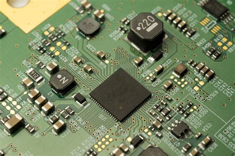
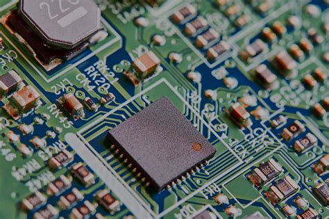
The PCB design and layout stage is where the foundation for a successful manufacturing process is laid. This stage involves creating a schematic diagram of the circuit, selecting appropriate components, and designing the physical layout of the PCB. The layout designer must consider factors such as component placement, routing, signal integrity, and manufacturability.
PCB Fabrication
Once the PCB layout is finalized, the design files are sent to a PCB fabrication facility. The fabrication process involves the following steps:
- Printing the circuit pattern onto a copper-clad laminate
- Etching away unwanted copper to create the desired circuit traces
- Drilling holes for component placement and vias
- Applying solder mask and silkscreen layers
A clean PCB layout ensures that the fabrication process runs smoothly, minimizing the risk of manufacturing defects and reducing the need for rework.
Component Placement and Soldering
After the PCB is fabricated, the next step is to place and solder the components onto the board. This process can be done manually or using automated pick-and-place machines. Proper component placement is crucial for both manual and automated assembly processes. A well-organized and clean PCB layout facilitates accurate component placement and reduces the chances of assembly errors.
Testing and Final Assembly
Once the components are soldered onto the PCB, the board undergoes various testing and inspection procedures to ensure proper functionality and quality. These tests may include visual inspections, automated optical inspections (AOI), and electrical tests. A clean PCB layout aids in the testing process by providing clear and easily accessible test points and minimizing the potential for short circuits or other issues.

Best Practices for PCB Layout Cleanup
To optimize your PCB layout for manufacturing, consider the following best practices:
1. Keep the Layout Organized and Symmetrical
A well-organized and symmetrical PCB layout not only improves the visual appearance but also enhances manufacturability. Group related components together and align them in a logical manner. Use consistent spacing and orientation for similar components. This helps in reducing assembly errors and makes the layout easier to understand for both designers and manufacturers.
2. Maintain Proper Clearances and Spacing
Ensuring adequate clearances and spacing between components, traces, and vias is crucial for manufacturing. Insufficient clearances can lead to short circuits, soldering issues, and reduced reliability. Consult with your PCB manufacturer to determine their minimum clearance requirements and design your layout accordingly. Consider factors such as component size, pad size, and trace width when determining the appropriate spacing.
3. Optimize Component Placement
Proper component placement is essential for efficient manufacturing and improved PCB performance. Consider the following guidelines when placing components:
- Place components in a logical flow, following the signal path whenever possible
- Minimize the distance between related components to reduce signal loss and interference
- Place decoupling capacitors close to their associated ICs to suppress noise
- Avoid placing components too close to the board edges to prevent damage during handling
- Consider the component height and placement for efficient soldering and accessibility
4. Route Traces Efficiently
Efficient trace routing is crucial for signal integrity and manufacturability. Follow these guidelines when routing traces:
- Keep trace lengths as short as possible to minimize signal loss and delay
- Avoid sharp angles and use 45-degree angles instead of 90-degree angles to reduce reflections
- Maintain consistent trace width and spacing for controlled impedance
- Use appropriate via sizes and placement to minimize signal degradation
- Avoid routing traces under components, especially those with high pin counts
5. Use Copper Pours and Ground Planes
Incorporating copper pours and ground planes in your PCB layout offers several benefits. Copper pours help in reducing electromagnetic interference (EMI) and provide a low-impedance return path for signals. Ground planes also improve signal integrity and provide shielding. When using copper pours and ground planes, ensure proper grounding and avoid creating isolated copper areas.
6. Implement Design for Manufacturing (DFM) Guidelines
Design for Manufacturing (DFM) guidelines are a set of best practices that ensure your PCB layout is optimized for manufacturing processes. These guidelines cover various aspects of PCB design, such as component placement, trace routing, solder mask application, and silkscreen legibility. Adhering to DFM guidelines helps in reducing manufacturing errors, improving yields, and lowering production costs.
Some key DFM guidelines include:
- Providing adequate clearances between components, traces, and board edges
- Using standardized component sizes and footprints
- Avoiding solder mask between pads and traces
- Ensuring silkscreen legibility and alignment with components
- Specifying appropriate solder mask and silkscreen colors
7. Perform Design Rule Checks (DRC)
Design Rule Checks (DRC) are automated checks performed by PCB design software to verify that your layout meets the specified design rules and constraints. These checks help in identifying potential issues such as clearance violations, short circuits, and missing connections. Running DRC on your PCB layout helps in catching errors early in the design process, reducing the risk of manufacturing issues and delays.
8. Collaborate with PCB Manufacturers
Effective collaboration with your PCB manufacturer is crucial for successful manufacturing. Engage with your manufacturer early in the design process and seek their input on design guidelines, material selection, and manufacturing capabilities. Provide clear and comprehensive documentation, including the PCB layout files, bill of materials (BOM), and assembly instructions. Maintain open communication with your manufacturer throughout the production process to address any issues promptly.

PCB Layout Cleanup Checklist
To ensure your PCB layout is optimized for manufacturing, use the following checklist:
- Components:
- [ ] Proper component placement and orientation
- [ ] Adequate clearances between components
- [ ] Decoupling capacitors placed close to ICs
-
[ ] Component heights considered for soldering and accessibility
-
Traces and Routing:
- [ ] Short and efficient trace routing
- [ ] Consistent trace width and spacing
- [ ] 45-degree angles used instead of 90-degree angles
- [ ] Traces not routed under components
-
[ ] Appropriate via sizes and placement
-
Copper Pours and Ground Planes:
- [ ] Copper pours used for EMI reduction and low-impedance return paths
- [ ] Ground planes implemented for signal integrity and shielding
-
[ ] Proper grounding and no isolated copper areas
-
DFM Guidelines:
- [ ] Adequate clearances between components, traces, and board edges
- [ ] Standardized component sizes and footprints used
- [ ] Solder mask applied correctly
- [ ] Silkscreen legibility and alignment with components
-
[ ] Appropriate solder mask and silkscreen colors specified
-
Design Rule Checks (DRC):
- [ ] DRC performed on the PCB layout
- [ ] Clearance violations, short circuits, and missing connections checked
-
[ ] Errors and warnings addressed
-
Documentation and Communication:
- [ ] Clear and comprehensive documentation provided to the manufacturer
- [ ] PCB layout files, BOM, and assembly instructions included
- [ ] Open communication maintained with the manufacturer
Benefits of PCB Layout Cleanup for Manufacturing
Investing time and effort into PCB layout cleanup offers several benefits for manufacturing:
-
Reduced Manufacturing Errors: A clean and optimized PCB layout minimizes the risk of manufacturing errors, such as short circuits, soldering issues, and component misplacements. This leads to higher yields and fewer rework cycles.
-
Improved Reliability: By adhering to best practices for component placement, trace routing, and clearances, you can enhance the reliability and longevity of your PCBs. A well-designed layout reduces the chances of signal integrity issues, EMI, and other potential problems.
-
Faster Production Time: A clean and organized PCB layout facilitates efficient manufacturing processes. With fewer errors and complications, the production time can be significantly reduced, allowing for faster time-to-market.
-
Cost Savings: PCB layout cleanup helps in reducing manufacturing costs in several ways. It minimizes the need for rework and repairs, reduces material waste, and optimizes the use of manufacturing resources. By catching and addressing issues early in the design process, you can avoid costly delays and iterations.
-
Enhanced Collaboration: Effective collaboration between PCB designers and manufacturers is crucial for successful manufacturing. A clean and well-documented PCB layout promotes better communication and understanding between the two parties. It helps in identifying and resolving potential issues early, leading to smoother production processes.
Frequently Asked Questions (FAQ)
-
Q: What is the importance of PCB layout cleanup for manufacturing?
A: PCB layout cleanup is crucial for manufacturing as it ensures proper functionality, minimizes errors, reduces production time, and lowers manufacturing costs. A clean and optimized layout facilitates efficient manufacturing processes and improves the reliability of the final product. -
Q: What are some key considerations when placing components on a PCB?
A: When placing components on a PCB, consider factors such as logical signal flow, distance between related components, placement of decoupling capacitors, component height, and accessibility for soldering. Proper component placement enhances manufacturability and improves PCB performance. -
Q: How can I ensure my PCB layout meets the manufacturer’s requirements?
A: To ensure your PCB layout meets the manufacturer’s requirements, adhere to their design guidelines, maintain proper clearances and spacing, use standardized component footprints, and follow DFM (Design for Manufacturing) best practices. Engage with your manufacturer early in the design process and seek their input on layout considerations. -
Q: What are Design Rule Checks (DRC) and why are they important?
A: Design Rule Checks (DRC) are automated checks performed by PCB design software to verify that your layout meets the specified design rules and constraints. DRC helps in identifying potential issues such as clearance violations, short circuits, and missing connections. Running DRC on your PCB layout helps in catching errors early, reducing the risk of manufacturing issues and delays. -
Q: How can I collaborate effectively with my PCB manufacturer?
A: Effective collaboration with your PCB manufacturer involves engaging with them early in the design process, seeking their input on design guidelines and manufacturing capabilities, providing clear and comprehensive documentation (including PCB layout files, BOM, and assembly instructions), and maintaining open communication throughout the production process. Foster a partnership approach to identify and resolve issues promptly.
Conclusion
PCB layout cleanup is a critical aspect of preparing your designs for efficient and successful manufacturing. By following best practices for component placement, trace routing, clearances, and adhering to DFM guidelines, you can optimize your PCB layout for manufacturability. A clean and well-organized layout reduces errors, improves reliability, saves time and costs, and enhances collaboration with manufacturers.
Remember to use the provided checklist to ensure your PCB layout is manufacturing-ready. Engage with your PCB manufacturer early in the design process and maintain open communication to address any issues promptly. By investing time and effort into PCB layout cleanup, you can streamline your manufacturing process, achieve higher yields, and deliver high-quality products to your customers.
No responses yet