What is PCB Layer Stack Up?
A PCB (Printed Circuit Board) layer stack up refers to the arrangement of copper layers and insulating materials that make up a PCB. It is a critical aspect of PCB design as it determines the electrical, mechanical, and thermal properties of the board. The layer stack up defines the number of layers, their order, thickness, and the materials used for each layer.
Why is PCB Layer Stack Up Important?
The PCB layer stack up plays a crucial role in the overall performance and reliability of the circuit board. Here are some reasons why it is important:
Signal integrity
The layer stack up can significantly impact the signal integrity of the PCB. By carefully selecting the layer order, thickness, and materials, designers can minimize signal interference, crosstalk, and noise. This is particularly important for high-speed designs where signal integrity is critical.
Impedance Control
The layer stack up also affects the characteristic impedance of the PCB traces. By controlling the trace width, thickness, and the distance between the trace and the reference plane, designers can achieve the desired impedance for each signal layer. This is essential for maintaining signal integrity and preventing reflections.
Power Distribution
The layer stack up determines how power and ground planes are distributed throughout the PCB. By strategically placing these planes, designers can minimize voltage drop, reduce electromagnetic interference (EMI), and improve overall power delivery to components.
Mechanical Strength
The choice of materials and the number of layers in the stack up can affect the mechanical strength of the PCB. Thicker boards with more layers tend to be more rigid and resistant to warping and bending. This is important for applications where the PCB is subjected to physical stress or vibrations.
Thermal Management
The layer stack up can also impact the thermal management of the PCB. By using materials with good thermal conductivity and strategically placing copper planes, designers can help dissipate heat generated by components more efficiently. This can prevent overheating and improve the overall reliability of the circuit.
Common PCB Layer Stack Ups
There are several common PCB layer stack ups used in the industry. Here are a few examples:
2-Layer PCB
A 2-layer PCB consists of a single core with copper layers on both sides. This is the simplest and most cost-effective stack up, suitable for low-complexity designs.
| Layer | Material | Thickness (mm) |
|---|---|---|
| Top Copper | Copper | 0.035 |
| Core | FR-4 | 1.6 |
| Bottom Copper | Copper | 0.035 |
4-Layer PCB
A 4-layer PCB has two additional copper layers, typically used for power and ground planes. This stack up provides better signal integrity and power distribution compared to a 2-layer board.
| Layer | Material | Thickness (mm) |
|---|---|---|
| Top Copper | Copper | 0.035 |
| Prepreg | FR-4 | 0.2 |
| Inner Layer 1 (Ground) | Copper | 0.035 |
| Core | FR-4 | 1.2 |
| Inner Layer 2 (Power) | Copper | 0.035 |
| Prepreg | FR-4 | 0.2 |
| Bottom Copper | Copper | 0.035 |
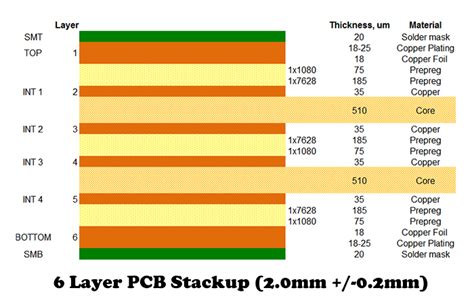
6-Layer PCB
A 6-layer PCB adds two more signal layers, providing even better signal integrity and routing flexibility. This stack up is commonly used for more complex designs with higher component density.
| Layer | Material | Thickness (mm) |
|---|---|---|
| Top Copper | Copper | 0.035 |
| Prepreg | FR-4 | 0.2 |
| Inner Layer 1 (Signal) | Copper | 0.035 |
| Core | FR-4 | 1.2 |
| Inner Layer 2 (Ground) | Copper | 0.035 |
| Core | FR-4 | 1.2 |
| Inner Layer 3 (Power) | Copper | 0.035 |
| Core | FR-4 | 1.2 |
| Inner Layer 4 (Signal) | Copper | 0.035 |
| Prepreg | FR-4 | 0.2 |
| Bottom Copper | Copper | 0.035 |

Factors to Consider When Choosing a PCB Layer Stack Up
When selecting a PCB layer stack up, designers must consider several factors to ensure the best performance and manufacturability. These factors include:
Design Requirements
The layer stack up should be chosen based on the specific requirements of the design, such as signal speed, component density, and power distribution needs. High-speed designs may require more layers and specialized materials to maintain signal integrity.
Cost
The number of layers and the materials used in the stack up can significantly impact the cost of the PCB. Generally, more layers and specialized materials will increase the cost. Designers must balance performance requirements with budget constraints.
Manufacturing Capabilities
The chosen layer stack up must be compatible with the manufacturing capabilities of the PCB fabricator. Some stack ups may require specialized equipment or processes that not all manufacturers can accommodate. It is important to consult with the fabricator early in the design process to ensure feasibility.
Material Properties
The properties of the materials used in the stack up, such as dielectric constant, loss tangent, and thermal conductivity, can affect the electrical and thermal performance of the PCB. Designers must carefully select materials based on the specific requirements of the application.
Reliability
The layer stack up can impact the long-term reliability of the PCB. Factors such as the glass transition temperature (Tg) of the materials, the coefficient of thermal expansion (CTE), and the adhesion between layers can affect the board’s ability to withstand environmental stresses over time.
Best Practices for Designing PCB Layer Stack Ups
To ensure optimal performance and manufacturability, designers should follow these best practices when designing PCB layer stack ups:
Use a Balanced Stack Up
A balanced stack up is symmetrical about the center layer, which helps prevent warping and twisting of the board during manufacturing. This is especially important for thicker boards with more layers.
Minimize the Number of Layers
While more layers can provide better signal integrity and routing flexibility, they also increase the cost and complexity of the PCB. Designers should use the minimum number of layers required to meet the design requirements.
Use Appropriate Trace Widths and Spacing
The trace width and spacing should be chosen based on the signal speed, current requirements, and manufacturability constraints. Designers should consult with the PCB fabricator to ensure that the chosen trace geometries are feasible.
Use Proper Via Design
Vias are used to connect traces between layers, but they can also introduce signal integrity issues if not designed properly. Designers should use appropriate via sizes and antipads, and avoid placing vias in sensitive areas such as under components or in high-speed signal paths.
Consider Signal Return Paths
For every signal trace, there must be a corresponding return path, typically on an adjacent ground or power plane. Designers should ensure that these return paths are continuous and uninterrupted to maintain signal integrity.
Use Copper Pours for Shielding
Copper pours on unused areas of the PCB can provide shielding against electromagnetic interference (EMI) and improve signal integrity. Designers should use copper pours on both sides of the board and connect them to ground or power planes as appropriate.
FAQ
1. What is the difference between a core and a prepreg in a PCB layer stack up?
A core is a solid, pre-cured laminate material that provides structural support for the PCB. Prepreg (pre-impregnated) is a partially cured material that is used to bond the layers together during the lamination process. Prepreg is typically thinner and more flexible than core material.
2. Can I use different materials for different layers in the stack up?
Yes, it is possible to use different materials for different layers in the stack up. For example, you may use a high-performance material for the high-speed signal layers and a standard material for the power and ground layers. However, this can increase the cost and complexity of the PCB.
3. What is the minimum number of layers required for a PCB?
The minimum number of layers required for a PCB is two (top and bottom). However, the actual number of layers needed depends on the complexity of the design, the number of components, and the signal and power requirements.
4. How does the layer stack up affect the impedance of the PCB traces?
The layer stack up can affect the impedance of the PCB traces in several ways. The thickness of the dielectric material between the trace and the reference plane, the width of the trace, and the properties of the dielectric material all contribute to the characteristic impedance of the trace. By carefully controlling these parameters, designers can achieve the desired impedance for each signal layer.
5. Can the PCB layer stack up affect the thermal performance of the board?
Yes, the PCB layer stack up can affect the thermal performance of the board. The choice of materials, the number of layers, and the placement of copper planes can all impact how heat is dissipated from the components. By using materials with good thermal conductivity and strategically placing copper planes, designers can help improve the thermal performance of the PCB.
Conclusion
The PCB layer stack up is a critical aspect of PCB design that can significantly impact the performance, reliability, and manufacturability of the circuit board. By carefully selecting the number of layers, their order, thickness, and materials, designers can optimize signal integrity, power distribution, mechanical strength, and thermal management.
When choosing a PCB layer stack up, designers must consider factors such as design requirements, cost, manufacturing capabilities, material properties, and long-term reliability. By following best practices such as using a balanced stack up, minimizing the number of layers, using appropriate trace geometries and via design, and considering signal return paths and shielding, designers can create high-quality PCBs that meet the specific needs of their applications.
No responses yet