Introduction to PCB Land Patterns and the IPC-7351 Standard
Printed Circuit Board (PCB) design is a complex process that involves various aspects, one of which is the creation of land patterns for components. A land pattern, also known as a footprint, is the arrangement of copper pads and holes on a PCB that allows for the soldering and electrical connection of a component to the board. Designing accurate and reliable land patterns is crucial for ensuring the proper functioning and longevity of electronic devices.
To standardize and optimize the design of PCB land patterns, the electronics industry relies on the IPC-7351 standard. Developed by the Association Connecting Electronics Industries (IPC), this standard provides guidelines and recommendations for the creation of land patterns for surface mount and through-hole components.
In this article, we will delve into the details of the IPC-7351 standard and explore its significance in PCB land pattern design. We will cover the key aspects of the standard, including land pattern dimensions, solder mask openings, and courtyard considerations. Additionally, we will discuss the benefits of adhering to the IPC-7351 standard and provide practical examples to illustrate its application in real-world PCB design scenarios.
Understanding the Key Components of a PCB Land Pattern
Before diving into the specifics of the IPC-7351 standard, it is essential to understand the basic components that make up a PCB land pattern. These components include:
-
Pads: Pads are the copper areas on a PCB that provide electrical contact points for soldering components. They are typically made of copper and coated with a thin layer of solder mask to prevent oxidation and improve solderability.
-
Holes: Holes are the openings drilled through the PCB to accommodate the leads of through-hole components or to provide mechanical support for surface mount components.
-
Solder Mask Opening: The solder mask opening is the area around the pads where the solder mask has been removed to expose the copper. This opening allows for proper soldering of the component to the pads.
-
Courtyard: The courtyard is an imaginary boundary that defines the maximum extent of the component on the PCB. It includes the pads, the component body, and any additional space required for assembly and inspection.
Understanding these components is crucial for designing effective PCB land patterns that comply with the IPC-7351 standard.
IPC-7351 Standard: Land Pattern Dimensions
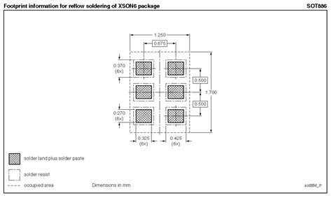
One of the primary focuses of the IPC-7351 standard is the specification of land pattern dimensions. The standard provides detailed guidelines for determining the appropriate sizes and shapes of pads and holes based on the component package type and size.
Pad Dimensions
The IPC-7351 standard defines three levels of density for pad dimensions: most, nominal, and least. These density levels correspond to different levels of component placement accuracy and manufacturing capabilities.
- Most density represents the smallest recommended pad dimensions, suitable for high-density designs and advanced manufacturing processes.
- Nominal density provides a balance between reliability and manufacturability, making it the most commonly used density level.
- Least density offers the largest pad dimensions, allowing for greater tolerances and easier assembly.
The standard provides tables and formulas for calculating the appropriate pad dimensions based on the component package type, size, and density level.
Hole Dimensions
For through-hole components, the IPC-7351 standard specifies the recommended hole sizes based on the lead diameter of the component. The standard provides a range of hole sizes to accommodate different lead diameters and plating thicknesses.
It is important to select the appropriate hole size to ensure a secure mechanical connection and reliable soldering of the component leads.

Solder Mask Openings and Solder Paste Considerations
In addition to pad and hole dimensions, the IPC-7351 standard also provides guidelines for solder mask openings and solder paste application.
Solder Mask Openings
The solder mask opening is the area around the pads where the solder mask has been removed to expose the copper. The size of the solder mask opening plays a crucial role in the soldering process and the reliability of the solder joint.
The IPC-7351 standard recommends solder mask opening sizes based on the component package type and the density level. The standard provides tables and formulas for calculating the appropriate solder mask opening dimensions.
It is important to ensure that the solder mask opening is large enough to allow for proper solder flow and wetting of the pads, while also preventing solder bridging between adjacent pads.
Solder Paste Application
Solder paste is a mixture of tiny solder particles suspended in a flux medium. It is applied to the pads prior to component placement and is responsible for forming the solder joint during the reflow soldering process.
The IPC-7351 standard provides recommendations for solder paste stencil aperture sizes and thickness based on the component package type and the pad dimensions. The standard aims to ensure an optimal amount of solder paste is deposited on the pads to achieve reliable solder joints.
It is crucial to follow the recommended solder paste application guidelines to prevent issues such as insufficient solder joint strength or excessive solder paste, which can lead to defects like solder bridging or tombstoning.
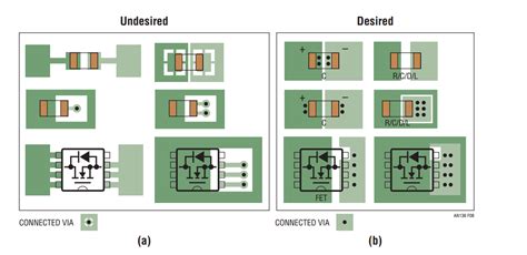
Courtyard Considerations in PCB Land Pattern Design
The courtyard is an imaginary boundary that defines the maximum extent of the component on the PCB. It encompasses the pads, the component body, and any additional space required for assembly and inspection.
The IPC-7351 standard provides guidelines for determining the appropriate courtyard dimensions based on the component package type and the assembly process requirements.
Courtyard Clearance
Courtyard clearance refers to the minimum distance between the courtyard boundary and any adjacent components or features on the PCB. The standard specifies the recommended courtyard clearance values to ensure adequate space for component placement, soldering, and inspection.
Maintaining proper courtyard clearance is essential for preventing physical interference between components and facilitating the assembly process. It also allows for easier rework and repair of the PCB if necessary.
Courtyard Marking
The IPC-7351 standard recommends marking the courtyard boundary on the PCB assembly drawing or the solder paste stencil drawing. This marking helps communicate the maximum extent of the component to the assembly team and ensures accurate placement during the manufacturing process.
The courtyard marking can be represented as a simple rectangular outline or a more detailed outline that follows the contours of the component body.
Benefits of Adhering to the IPC-7351 Standard
Designing PCB land patterns in accordance with the IPC-7351 standard offers several benefits for both designers and manufacturers:
-
Consistency and Reliability: By following the standard guidelines, designers can create land patterns that are consistent and reliable across different projects and manufacturing facilities. This consistency reduces the likelihood of assembly issues and improves the overall quality of the PCB.
-
Compatibility with Manufacturing Processes: The IPC-7351 standard takes into account the capabilities and limitations of various manufacturing processes, such as solder paste printing and component placement. Adhering to the standard ensures that the land patterns are compatible with these processes, minimizing the risk of defects and improving yield.
-
Reduced Design Time: The standard provides a set of well-defined guidelines and formulas for calculating land pattern dimensions. This eliminates the need for designers to perform extensive calculations or rely on trial and error, thereby reducing the overall design time.
-
Improved Communication: By using a common standard, designers and manufacturers can communicate more effectively. The standard provides a shared language and understanding of land pattern requirements, reducing the potential for misinterpretation and errors.
-
Enhanced Reliability: Properly designed land patterns based on the IPC-7351 standard contribute to the overall reliability of the PCB. The standard ensures adequate pad sizes, solder mask openings, and courtyard clearances, which promote robust solder joints and minimize the risk of component failures.
Practical Examples of IPC-7351 Standard Application
To illustrate the application of the IPC-7351 standard in real-world scenarios, let’s consider a few practical examples:
Example 1: Designing a Land Pattern for a QFN Package
Suppose you need to design a land pattern for a QFN (Quad Flat No-lead) package with dimensions of 5mm x 5mm and a pitch of 0.5mm. Using the IPC-7351 standard, you can follow these steps:
-
Determine the density level based on your design requirements and manufacturing capabilities. Let’s assume you choose the nominal density level.
-
Refer to the IPC-7351 standard tables or use the provided formulas to calculate the recommended pad dimensions for the QFN package at the nominal density level.
-
Design the land pattern in your PCB design software, using the calculated pad dimensions and the recommended solder mask opening sizes from the standard.
-
Define the courtyard boundary around the land pattern, ensuring sufficient clearance for assembly and inspection based on the standard guidelines.
-
Include the courtyard marking in the PCB assembly drawing or solder paste stencil drawing to communicate the component’s maximum extent to the manufacturing team.
By following these steps and adhering to the IPC-7351 standard, you can create a reliable and manufacturable land pattern for the QFN package.
Example 2: Optimizing Solder Paste Stencil Aperture for a BGA Package
When working with a BGA (Ball Grid Array) package, the solder paste stencil aperture design is crucial for achieving reliable solder joints. The IPC-7351 standard provides recommendations for stencil aperture dimensions based on the pad size and pitch.
Let’s assume you have a BGA package with a pad diameter of 0.5mm and a pitch of 1mm. To optimize the solder paste stencil aperture, follow these steps:
-
Consult the IPC-7351 standard tables or use the provided formulas to determine the recommended stencil aperture dimensions for the given pad size and pitch.
-
Design the stencil aperture in your PCB design software or provide the necessary information to your stencil manufacturer.
-
Specify the stencil thickness based on the standard recommendations, taking into account the solder paste volume requirements for the BGA package.
-
Verify that the designed stencil aperture allows for sufficient solder paste deposition on the pads while preventing excessive solder paste that could lead to defects.
By optimizing the solder paste stencil aperture according to the IPC-7351 standard, you can ensure reliable solder joints and improve the assembly yield for the BGA package.
Frequently Asked Questions (FAQ)
-
What is the IPC-7351 standard?
The IPC-7351 standard is a set of guidelines and recommendations developed by the Association Connecting Electronics Industries (IPC) for the design of PCB land patterns. It provides specifications for pad dimensions, solder mask openings, and courtyard considerations to ensure reliable and manufacturable PCB assemblies. -
Why is it important to follow the IPC-7351 standard in PCB land pattern design?
Following the IPC-7351 standard in PCB land pattern design offers several benefits, including: - Consistency and reliability across different projects and manufacturing facilities
- Compatibility with manufacturing processes, reducing the risk of defects
- Reduced design time by providing well-defined guidelines and formulas
- Improved communication between designers and manufacturers
-
Enhanced reliability of the PCB assembly
-
What are the different density levels defined in the IPC-7351 standard?
The IPC-7351 standard defines three density levels for pad dimensions: - Most density: Represents the smallest recommended pad dimensions, suitable for high-density designs and advanced manufacturing processes.
- Nominal density: Provides a balance between reliability and manufacturability, being the most commonly used density level.
-
Least density: Offers the largest pad dimensions, allowing for greater tolerances and easier assembly.
-
How does the IPC-7351 standard address solder mask openings?
The IPC-7351 standard provides guidelines for solder mask opening sizes based on the component package type and the density level. It recommends solder mask opening dimensions that allow for proper solder flow and wetting of the pads while preventing solder bridging between adjacent pads. -
What is the purpose of the courtyard in PCB land pattern design?
The courtyard is an imaginary boundary that defines the maximum extent of the component on the PCB. It includes the pads, the component body, and any additional space required for assembly and inspection. The IPC-7351 standard provides guidelines for determining the appropriate courtyard dimensions and clearances to ensure adequate space for component placement, soldering, and inspection.
Conclusion
The IPC-7351 standard is a valuable resource for PCB designers and manufacturers, providing comprehensive guidelines and recommendations for the design of PCB land patterns. By adhering to this standard, designers can create land patterns that are consistent, reliable, and compatible with manufacturing processes.
Throughout this article, we have explored the key aspects of the IPC-7351 standard, including land pattern dimensions, solder mask openings, and courtyard considerations. We have discussed the benefits of following the standard, such as improved consistency, reduced design time, and enhanced reliability.
Furthermore, we have provided practical examples to illustrate the application of the standard in real-world scenarios, such as designing a land pattern for a QFN package and optimizing the solder paste stencil aperture for a BGA package.
By understanding and implementing the IPC-7351 standard in your PCB land pattern design process, you can ensure the creation of high-quality, manufacturable PCB assemblies. This standard serves as a foundation for effective communication between designers and manufacturers, ultimately leading to improved product reliability and customer satisfaction.
As PCB technology continues to evolve, the IPC-7351 standard will remain a crucial resource for the electronics industry, guiding the design and manufacturing of reliable and efficient electronic devices.
No responses yet