
Introduction to PCB Stackups and Ground Planes
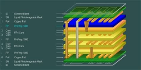
A printed circuit board (PCB) stackup refers to the arrangement of copper and insulating layers that make up a PCB. The stackup is one of the most critical aspects of PCB design, as it determines the board’s electrical properties, signal integrity, power distribution, and mechanical strength.
In a typical PCB stackup, the layers alternate between signal layers and planes. Signal layers route traces that carry signals between components, while plane layers are used for power distribution and grounding. A solid copper pour that spans most of the PCB area is known as a ground plane.
Ground planes serve several important functions in a PCB:
- Providing a low-impedance return path for signals
- Reducing electromagnetic interference (EMI) and crosstalk
- Improving signal integrity and power integrity
- Providing shielding and preventing signal coupling
To achieve optimal performance, it is crucial to follow best practices when designing ground planes in your multilayer PCB stackup. This article will delve into the key considerations and guidelines for implementing effective ground planes.
Signal Return Paths and Ground Plane Placement
One of the primary roles of a ground plane is to provide a low-impedance return path for signals. When a signal travels along a trace, it induces a return current that flows through the ground plane beneath it. The return current follows the path of least impedance, which is typically directly under the signal trace.
To ensure a clean and efficient return path, it is essential to place ground planes adjacent to signal layers. This proximity minimizes the loop area between the signal trace and its return path, reducing inductance and electromagnetic emissions.
Best practices for ground plane placement in a multilayer stackup:
- Place a ground plane next to each signal layer, either above or below it.
- For high-speed signals, prioritize placing the ground plane closest to the signal layer to minimize loop area.
- Use symmetrical stackups whenever possible, with equal numbers of signal layers and ground planes on each side of the board center.
Example 4-layer stackup with proper ground plane placement:
| Layer | Type |
|---|---|
| Top | Signal |
| L2 | Ground Plane |
| L3 | Power Plane |
| Bottom | Signal |
In this stackup, each signal layer has an adjacent ground plane, ensuring clean return paths and minimizing EMI.
Ground Plane Stitching and Via Placement
While ground planes provide a continuous return path within each layer, it is also important to maintain continuity between ground planes on different layers. This is achieved through proper via placement and ground plane stitching.
Ground plane stitching involves placing vias at regular intervals to connect ground planes on different layers. This creates a low-impedance path for return currents to flow between layers, minimizing differences in ground potential and reducing EMI.
Best practices for ground plane stitching and via placement:
- Place ground stitching vias at regular intervals, typically every 1/20th to 1/10th of a wavelength of the highest frequency signal.
- Use a via spacing of no more than 100 mils (2.54 mm) for most designs.
- Place ground stitching vias near the edges of the board and around high-current or noise-sensitive areas.
- Ensure that signal vias have a nearby ground via to provide a return path between layers.
Example via placement for ground plane stitching:
    o   o   o   o   o
     o   o   o   o
    o   o   o   o   o
     o   o   o   o
    o   o   o   o   o
In this example, ground stitching vias (represented by ‘o’) are placed in a regular grid pattern, ensuring a low-impedance connection between ground planes on different layers.

Split Ground Planes and Partitioning
In some cases, it may be necessary to create separate ground planes for different sections of a PCB. This is known as ground plane splitting or partitioning. Split ground planes are used to isolate noise-sensitive circuits from noisy circuits, prevent ground loops, or accommodate different voltage levels.
When splitting ground planes, it is important to maintain a single point of connection between the planes, known as a star ground or ground tie-point. This prevents ground loops and ensures that return currents have a well-defined path.
Best practices for split ground planes and partitioning:
- Identify circuits that require isolation, such as analog and digital sections, or high-current and low-current areas.
- Create separate ground planes for each section, with a single point of connection (star ground) between them.
- Place the star ground connection near the power supply or voltage regulator, where the different ground references originate.
- Use a small trace or resistor (0.1 to 10 ohms) to connect the star ground to the main ground plane, limiting noise coupling between sections.
Example split ground plane layout:
+-------+     +-------+
|       |     |       |
| Analog|     |Digital|
|  GND  |     |  GND  |
|       |     |       |
+-------+     +-------+
     |            |
     +-----+------+
           |
       Star Ground
In this example, separate ground planes are used for the analog and digital sections of the PCB, with a star ground connection joining them at a single point.
Ground Plane Cutouts and Clearances
While ground planes provide many benefits, there are situations where it is necessary to create cutouts or clearances in the ground plane. Cutouts are used to accommodate component placement, provide isolation, or allow for mechanical features such as mounting holes or connectors.
When creating cutouts in a ground plane, it is important to minimize their size and maintain sufficient clearance around sensitive traces or components. Large cutouts can disrupt the flow of return currents and increase inductance, leading to signal integrity issues.
Best practices for ground plane cutouts and clearances:
- Keep cutouts as small as possible, ideally no larger than the component or feature they accommodate.
- Maintain a minimum clearance of 20 mils (0.508 mm) between the edge of a cutout and any sensitive traces or components.
- Avoid creating cutouts that run parallel to high-speed traces, as this can cause discontinuities in the return path.
- Use stitching vias around the perimeter of large cutouts to maintain ground plane continuity.
Example ground plane cutout with stitching vias:
    +-----------+
    |           |
    |  Cutout   |
    |           |
    +-----o-----+
          o
    +-----o-----+
    |           |
    |           |
    |           |
    +-----------+
In this example, a ground plane cutout is surrounded by stitching vias (represented by ‘o’) to maintain continuity and minimize the impact on return currents.
High-Frequency Considerations and Skin Effect
At high frequencies, the behavior of ground planes becomes more complex due to the skin effect and the formation of standing waves. The skin effect causes current to flow primarily on the surface of a conductor, reducing the effective cross-sectional area and increasing impedance.
To mitigate the impact of the skin effect, it is important to maintain a sufficient ground plane thickness and to use appropriate materials. The skin depth, which is the distance that current penetrates into a conductor, decreases with increasing frequency.
Best practices for high-frequency ground plane design:
- Use a ground plane thickness of at least 3 to 5 times the skin depth at the maximum operating frequency.
- For frequencies above 1 GHz, consider using low-loss materials such as Rogers or Isola laminates.
- Minimize the use of vias in high-frequency signal paths, as they can cause discontinuities and reflections.
- Use ground plane stitching to create a tightly-coupled mesh that minimizes impedance and suppresses standing waves.
Example skin depth calculation:
At 1 GHz, the skin depth of copper is approximately 2.1 microns (0.0021 mm). To ensure a low-impedance ground plane, the copper thickness should be at least 6.3 to 10.5 microns (0.0063 to 0.0105 mm).
Power Plane Considerations and Decoupling
In addition to ground planes, multilayer PCBs often incorporate power planes for distributing supply voltages to components. Power planes provide a low-impedance source of current and help to reduce voltage ripple and noise.
To ensure a clean and stable power supply, it is important to use appropriate decoupling techniques in conjunction with power planes. Decoupling capacitors placed near ICs help to filter high-frequency noise and provide local energy storage.
Best practices for power plane design and decoupling:
- Place power planes close to the ground plane to minimize inductance and provide a low-impedance return path.
- Use a solid copper pour for power planes, with a minimum copper weight of 1 oz/ft² (35 microns).
- Locate decoupling capacitors as close to IC power pins as possible, ideally within 100 mils (2.54 mm).
- Use a combination of bulk, ceramic, and small-package capacitors to provide a range of decoupling frequencies.
- Provide separate power planes for analog and digital circuits to minimize noise coupling.
Example decoupling capacitor placement:
       +-------+
       |       |
     --+---+   |
     | C  |   |
  ---|    |   |
 +---|    |   |
 |VCC| IC |GND|
 +---|    |   |
  ---|    |   |
     |    |   |
     |-+--+   |
      GND |   |
       |  |   |
       +--+---+
In this example, a decoupling capacitor (C) is placed close to the power (VCC) and ground (GND) pins of an IC, minimizing the loop area and providing effective high-frequency decoupling.
Grounding in Mixed-Signal PCBs
Designing ground planes for mixed-signal PCBs, which contain both analog and digital circuits, presents additional challenges. Analog circuits are sensitive to noise, while digital circuits generate significant amounts of switching noise. Proper grounding techniques are essential to maintain signal integrity and prevent interference between the two domains.
Best practices for grounding in mixed-signal PCBs:
- Use separate ground planes for analog and digital circuits, with a single point of connection (star ground) between them.
- Place the star ground connection near the ADC or DAC, where the analog and digital domains interface.
- Route analog and digital traces on separate layers, with their respective ground planes beneath them.
- Use ground plane cutouts or guard rings to isolate sensitive analog circuits from digital noise.
- Implement proper decoupling and filtering techniques for both analog and digital power supplies.
Example mixed-signal PCB stackup:
| Layer | Type |
|---|---|
| Top | Analog Signal |
| L2 | Analog Ground |
| L3 | Digital Ground |
| L4 | Digital Signal |
| L5 | Power Plane |
| Bottom | Digital Signal |
In this stackup, separate ground planes are used for the analog and digital sections, with the power plane placed between them. This arrangement helps to isolate the sensitive analog circuits from digital noise.
FAQ
-
What is a ground plane in a PCB?
A ground plane is a large area of copper that covers most of the PCB surface on one or more layers. It provides a low-impedance return path for signals, helps to reduce EMI and crosstalk, and improves signal and power integrity. -
Why are ground planes important in a multilayer PCB stackup?
Ground planes are crucial in multilayer PCBs because they provide a reference for signals, enable proper return paths, and help to control impedance. They also offer shielding between layers and prevent unwanted coupling between signals. -
How do I determine the optimal ground plane placement in my stackup?
The optimal ground plane placement depends on the specific requirements of your design. As a general rule, place a ground plane adjacent to each signal layer, either above or below it. For high-speed signals, prioritize placing the ground plane closest to the signal layer to minimize loop area and inductance. -
What is ground plane stitching, and why is it necessary?
Ground plane stitching involves placing vias at regular intervals to connect ground planes on different layers. It is necessary to maintain continuity between ground planes, create a low-impedance path for return currents, and minimize differences in ground potential across the PCB. -
How do I handle grounding in a mixed-signal PCB?
When designing a mixed-signal PCB, use separate ground planes for analog and digital circuits, with a single point of connection (star ground) between them. Place the star ground near the ADC or DAC, where the analog and digital domains interface. Use proper isolation techniques, such as ground plane cutouts or guard rings, to protect sensitive analog circuits from digital noise.
By following these best practices and guidelines, you can design effective ground planes in your multilayer PCB stackup, ensuring optimal signal integrity, power distribution, and EMI control. Remember to consider the specific requirements of your design and adapt these techniques accordingly.
No responses yet