Introduction to PCB Testing
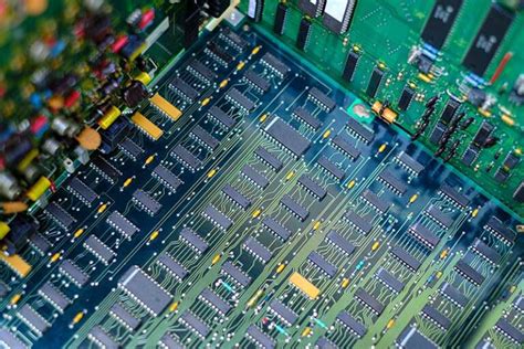
Printed Circuit Board (PCB) testing is a crucial step in the electronics manufacturing process to ensure the quality, reliability, and functionality of the end product. PCB testing involves various methods and techniques to verify that the manufactured PCB meets the design specifications and functions as intended.
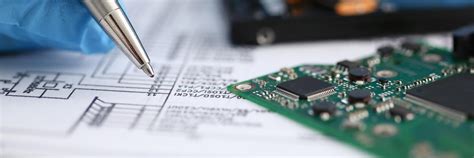
Effective collaboration between the PCB designer, manufacturer, and testing team is essential for successful PCB testing and to minimize issues and delays in the production process. In this article, we will explore the importance of PCB functional testing, the different types of tests involved, and the role of collaboration between stakeholders.
Types of PCB Testing
PCB testing can be broadly categorized into two types: functional testing and non-functional testing.
Functional Testing
Functional testing, also known as system-level testing, involves verifying that the PCB performs its intended functions as per the design specifications. This type of testing focuses on the PCB’s behavior and its interaction with other components in the system. Some common functional tests include:
- Power-on testing
- Boundary scan testing
- In-circuit testing
- Functional test
- Burn-in testing
Non-Functional Testing
Non-functional testing, on the other hand, involves testing the PCB’s physical and chemical properties, such as:
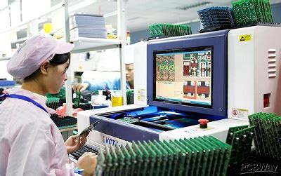
- Visual inspection
- Automated Optical Inspection (AOI)
- X-ray inspection
- Microsectioning
- Solderability testing
- Contamination testing
Importance of PCB Functional Testing
PCB functional testing is essential to ensure that the manufactured PCB meets the design intent and functions reliably in the end product. Some key reasons why functional testing is crucial are:
- Verifying design functionality
- Identifying manufacturing defects
- Ensuring reliability and durability
- Meeting regulatory and compliance requirements
- Reducing field failures and warranty claims

Role of Manufacturer Collaboration in PCB Testing
Effective collaboration between the PCB designer, manufacturer, and testing team is vital for successful PCB testing. Each stakeholder plays a critical role in ensuring that the PCB is designed, manufactured, and tested to meet the required specifications and quality standards.
PCB Designer’s Role
The PCB designer is responsible for creating a design that is manufacturable, testable, and meets the functional requirements. Some key considerations for the designer include:
- Designing for manufacturability (DFM)
- Designing for testability (DFT)
- Providing clear and comprehensive design documentation
- Collaborating with the manufacturer and testing team to address any design issues
PCB Manufacturer’s Role
The PCB manufacturer is responsible for fabricating the PCB according to the design specifications and ensuring that it meets the required quality standards. Some key responsibilities of the manufacturer include:
- Reviewing the design files for manufacturability
- Selecting the appropriate materials and processes
- Implementing quality control measures
- Collaborating with the designer and testing team to resolve any manufacturing issues
Testing Team’s Role
The testing team is responsible for developing and executing the test plan to verify the PCB’s functionality and quality. Some key tasks of the testing team include:
- Developing the test strategy and test cases
- Setting up the test environment and equipment
- Executing the functional and non-functional tests
- Analyzing the test results and providing feedback to the designer and manufacturer
Best Practices for Effective PCB Testing Collaboration
To ensure effective collaboration between the PCB designer, manufacturer, and testing team, some best practices include:
- Early involvement of all stakeholders in the design process
- Clear communication and documentation of requirements and specifications
- Regular design reviews and feedback loops
- Adequate testing coverage and test planning
- Continuous improvement and lessons learned analysis
FAQ
Q1. What is the difference between functional and non-functional PCB testing?
A1. Functional testing focuses on verifying that the PCB performs its intended functions as per the design specifications, while non-functional testing involves testing the PCB’s physical and chemical properties, such as visual inspection, AOI, X-ray, and solderability testing.
Q2. Why is PCB functional testing important?
A2. PCB functional testing is essential to ensure that the manufactured PCB meets the design intent, functions reliably in the end product, identifies manufacturing defects, ensures compliance with regulations, and reduces field failures and warranty claims.
Q3. What are some common functional tests performed on PCBs?
A3. Some common functional tests performed on PCBs include power-on testing, boundary scan testing, in-circuit testing, functional testing, and burn-in testing.
Q4. What is the role of the PCB designer in the testing process?
A4. The PCB designer is responsible for creating a design that is manufacturable, testable, and meets the functional requirements. They should design for manufacturability (DFM) and testability (DFT), provide clear design documentation, and collaborate with the manufacturer and testing team to address any design issues.
Q5. How can effective collaboration between stakeholders improve PCB testing?
A5. Effective collaboration between the PCB designer, manufacturer, and testing team can improve PCB testing by ensuring early involvement of all stakeholders, clear communication of requirements, regular design reviews and feedback, adequate test coverage, and continuous improvement through lessons learned analysis.
Conclusion
PCB functional testing is a critical step in the electronics manufacturing process to ensure the quality, reliability, and functionality of the end product. Effective collaboration between the PCB designer, manufacturer, and testing team is essential for successful PCB testing and to minimize issues and delays in the production process.
By understanding the different types of PCB testing, the importance of functional testing, and the roles and responsibilities of each stakeholder, companies can implement best practices for effective collaboration and improve the overall quality and efficiency of their PCB testing process.
| Stakeholder | Key Responsibilities |
|---|---|
| PCB Designer | – Design for manufacturability (DFM) and testability (DFT) – Provide clear design documentation – Collaborate with manufacturer and testing team |
| PCB Manufacturer | – Review design files for manufacturability – Select appropriate materials and processes – Implement quality control measures – Collaborate with designer and testing team |
| Testing Team | – Develop test strategy and test cases – Set up test environment and equipment – Execute functional and non-functional tests – Analyze test results and provide feedback |
Table 1: Key responsibilities of PCB testing stakeholders
By fostering a culture of collaboration and continuous improvement, companies can enhance their PCB testing process, reduce defects and failures, and ultimately deliver high-quality and reliable electronic products to their customers.
No responses yet