Introduction to PCB Etching
PCB etching is a critical process in the manufacturing of printed circuit boards (PCBs). It involves selectively removing unwanted copper from a copper-clad substrate to create the desired circuit pattern. The resulting PCB serves as the foundation for electronic components and provides electrical connectivity in electronic devices.
In this comprehensive article, we will delve into the intricacies of PCB etching services, exploring the various techniques, benefits, and considerations involved in this essential aspect of PCB fabrication.
Understanding the PCB Etching Process
Step 1: PCB Design and Preparation
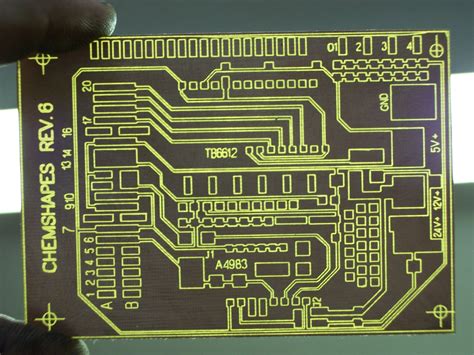
The PCB etching process begins with the design of the circuit board. Using specialized PCB design software, engineers create a digital layout of the desired circuit pattern. This design is then transferred onto the copper-clad substrate through a process called “resist application.”
Resist application involves coating the copper surface with a light-sensitive material known as photoresist. The photoresist can be applied through various methods, such as screen printing, roller coating, or spray coating.
Step 2: Exposure and Development
Once the photoresist is applied, the PCB undergoes exposure to UV light. The PCB design artwork, which is typically a photographic film or glass master, is placed on top of the photoresist-coated copper surface. UV light is then shone through the artwork, selectively hardening the exposed areas of the photoresist.
After exposure, the PCB is subjected to a development process. The unexposed areas of the photoresist are dissolved using a chemical developer solution, revealing the bare copper underneath. The exposed and hardened areas of the photoresist remain intact, protecting the copper that will form the circuit pattern.
Step 3: Etching
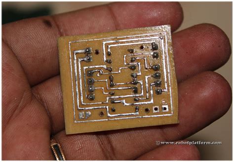
With the desired circuit pattern now exposed, the PCB is ready for etching. The etching process removes the unwanted copper from the substrate, leaving only the protected copper traces that form the circuit pattern.
There are two primary methods of PCB etching:
-
Chemical Etching: In chemical etching, the PCB is immersed in an etchant solution, typically ferric chloride or ammonium persulfate. The etchant chemically reacts with the exposed copper, dissolving it and leaving the protected copper intact. Chemical etching is widely used due to its simplicity and cost-effectiveness.
-
Plasma Etching: Plasma etching, also known as dry etching, uses a plasma (ionized gas) to remove the unwanted copper. The PCB is placed in a vacuum chamber, and a reactive gas is introduced. The gas is ionized using radio frequency (RF) energy, creating a plasma. The plasma reacts with the exposed copper, etching it away while leaving the protected copper unaffected. Plasma etching offers high precision and is often used for fine-pitch and high-density PCBs.
Step 4: Resist Removal and Finishing
After etching, the remaining photoresist is stripped away using a chemical stripper or through mechanical abrasion. This step reveals the final etched circuit pattern on the PCB.
Finally, the PCB undergoes various finishing processes to enhance its functionality and durability. These processes may include:
- Solder mask application: A protective layer is applied to the PCB to prevent accidental short circuits and improve solderability.
- Silkscreen printing: Text, symbols, and component designators are printed onto the PCB for easy identification and assembly.
- Surface finish: A surface finish, such as immersion silver, immersion tin, or gold plating, is applied to the exposed copper to prevent oxidation and enhance solderability.
Advantages of Professional PCB Etching Services
While it is possible to etch PCBs in-house, utilizing professional PCB etching services offers several advantages:
1. Quality and Precision
Professional PCB etching services have access to state-of-the-art equipment and skilled technicians who specialize in the etching process. They can achieve high levels of precision and ensure consistent quality across multiple PCBs. This is particularly important for complex designs with fine traces and tight tolerances.
2. Faster Turnaround Times
PCB etching service providers have streamlined processes and dedicated resources to handle high volumes of PCB orders efficiently. They can often deliver etched PCBs faster than in-house etching, reducing overall project timelines.
3. Cost-Effectiveness
Outsourcing PCB etching to a professional service can be more cost-effective than setting up and maintaining an in-house etching facility. Service providers benefit from economies of scale, allowing them to offer competitive pricing without compromising on quality.
4. Access to Advanced Technologies
Professional PCB etching services invest in the latest technologies and processes to stay competitive in the market. They can offer advanced etching techniques, such as plasma etching, which may not be feasible or cost-effective for in-house operations.
5. Compliance with Industry Standards
Reputable PCB etching service providers adhere to industry standards and regulations, ensuring that the etched PCBs meet the required specifications and quality criteria. They often have certifications such as ISO 9001 and IPC standards, demonstrating their commitment to quality and reliability.

Choosing the Right PCB Etching Service
When selecting a PCB etching service provider, consider the following factors:
1. Experience and Expertise
Look for a service provider with extensive experience in PCB etching and a proven track record of delivering high-quality results. Consider their expertise in handling different PCB materials, design complexities, and etching techniques.
2. Capabilities and Technologies
Evaluate the service provider’s capabilities and the technologies they employ. Ensure they have the necessary equipment and processes to handle your specific PCB etching requirements, such as fine-pitch etching, controlled impedance, or special materials.
3. Turnaround Time and Delivery
Inquire about the service provider’s typical turnaround times and their ability to meet your project deadlines. Consider their location and delivery options to ensure timely receipt of the etched PCBs.
4. Quality Control and Certifications
Assess the service provider’s quality control measures and certifications. Look for certifications such as ISO 9001, IPC standards, and any industry-specific certifications relevant to your project. A robust quality control system ensures consistent and reliable results.
5. Customer Support and Communication
Choose a service provider that offers responsive customer support and clear communication channels. They should be able to address your queries, provide technical assistance, and keep you informed throughout the etching process.
PCB Etching Techniques Comparison
| Technique | Advantages | Disadvantages |
|---|---|---|
| Chemical Etching | – Simple and cost-effective – Widely available – Suitable for most PCB designs |
– Limited resolution compared to plasma etching – Requires careful handling of chemicals |
| Plasma Etching | – High precision and resolution – Suitable for fine-pitch and high-density PCBs – Environmentally friendly |
– Higher cost compared to chemical etching – Requires specialized equipment and expertise |
FAQ
1. What is the minimum feature size achievable with PCB etching?
The minimum feature size achievable with PCB etching depends on the etching technique used. Chemical etching can typically achieve feature sizes down to 0.1 mm (4 mil), while plasma etching can achieve even smaller feature sizes, often below 0.05 mm (2 mil).
2. How long does the PCB etching process take?
The PCB etching process duration varies depending on factors such as the PCB size, complexity, and the etching technique employed. Chemical etching typically takes anywhere from a few minutes to an hour, while plasma etching may take longer due to the additional setup and processing time.
3. Can PCB etching services handle multilayer PCBs?
Yes, professional PCB etching services can handle multilayer PCBs. The etching process is repeated for each layer of the PCB, and the layers are aligned and laminated together to form the final multilayer PCB.
4. What materials can be etched using PCB etching services?
PCB etching services commonly work with copper-clad substrates such as FR-4, polyimide, and flexible materials like Kapton. They can also handle specialized substrates like aluminum or copper-clad ceramics, depending on their capabilities.
5. How do I prepare my PCB design files for etching?
When preparing your PCB design files for etching, ensure that you provide the files in a standard format such as Gerber or ODB++. Include all the necessary layers, such as the copper layers, solder mask, and silkscreen. Consult with your PCB etching service provider for specific file requirements and design guidelines.
Conclusion
PCB etching is a critical process in the fabrication of printed circuit boards, enabling the creation of precise and reliable circuit patterns. By understanding the PCB etching process, its advantages, and the factors to consider when choosing a PCB etching service, you can ensure the successful production of high-quality PCBs for your electronic projects.
Partnering with a reputable PCB etching service provider offers access to advanced technologies, expertise, and cost-effective solutions, allowing you to focus on your core competencies while leaving the etching process in capable hands.
As technology continues to advance and electronic devices become increasingly complex, the importance of reliable and precise PCB etching services will only grow. By staying informed and making informed decisions, you can leverage the power of PCB etching to bring your innovative designs to life.
No responses yet