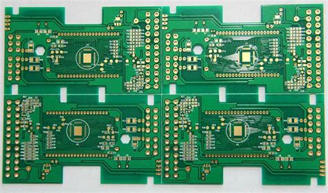
Introduction to PCB Etching
Printed Circuit Board (PCB) etching is a crucial process in the manufacturing of electronic circuits. It involves the removal of unwanted copper from a PCB substrate to create the desired circuit pattern. The etching process can be done using various methods, but the most common ones are chemical etching and mechanical etching.
In this article, we will explore the different aspects of PCB etching, including the materials and equipment required, the steps involved in the etching process, and the best practices for achieving perfect PCB etching.
Materials and Equipment Required for PCB Etching
To perform PCB etching, you will need the following materials and equipment:
- PCB substrate (copper-clad board)
- Etchant solution (ferric chloride or ammonium persulfate)
- Etching tank or container
- Protective gloves and eyewear
- Maskant (resist ink or dry film photoresist)
- Exposure unit (for photoresist)
- Developer solution (for photoresist)
- Drill or CNC machine (for drilling holes)
PCB Substrate
The PCB substrate is the base material on which the circuit pattern is etched. It consists of a non-conductive material, such as fiberglass or phenolic resin, coated with a thin layer of copper on one or both sides. The thickness of the copper layer can vary depending on the application, but it typically ranges from 0.5 oz to 2 oz per square foot.
Etchant Solution
The etchant solution is the chemical used to remove the unwanted copper from the PCB substrate. The two most common etchants are ferric chloride (FeCl3) and ammonium persulfate ((NH4)2S2O8). Ferric chloride is more widely used due to its lower cost and easier handling, but ammonium persulfate is preferred for its faster etching rate and cleaner results.
Etching Tank or Container
The etching tank or container is where the actual etching process takes place. It should be made of a material that is resistant to the etchant solution, such as plastic or glass. The size of the tank will depend on the size of the PCBs being etched, but it should be large enough to accommodate the PCB and allow for sufficient circulation of the etchant solution.
Protective Gear
PCB etching involves the use of hazardous chemicals, so it is essential to wear protective gloves and eyewear to avoid skin contact and eye injury. Nitrile gloves are recommended for their chemical resistance, and safety glasses or goggles should be worn to protect the eyes from splashes or fumes.
Maskant
The maskant is a material used to protect the areas of the PCB that should not be etched. It can be in the form of a resist ink or a dry film photoresist. Resist ink is applied manually using a pen or brush, while photoresist is applied as a film and exposed to UV light to create the desired pattern.
Exposure Unit
An exposure unit is required when using photoresist as the maskant. It consists of a UV light source and a vacuum frame to hold the PCB and photoresist in place during exposure. The exposure time and intensity will depend on the type of photoresist used and the desired pattern.
Developer Solution
After exposure, the photoresist needs to be developed to remove the unexposed areas and reveal the circuit pattern. The developer solution is typically a weak alkaline solution, such as sodium carbonate or potassium carbonate.
Drill or CNC Machine
Once the PCB is etched, holes need to be drilled for component leads and mounting. This can be done manually using a drill press or automatically using a CNC machine. The drill bits used should be of the appropriate size and material for the PCB substrate and the components being used.

Steps Involved in PCB Etching
The PCB etching process involves several steps, which are outlined below:
Step 1: PCB Design and Artwork Preparation
The first step in PCB etching is to design the circuit and create the artwork for the PCB. This can be done using PCB design software, such as Eagle, KiCad, or Altium Designer. The artwork should include the circuit pattern, component footprints, and any text or graphics required.
Step 2: Transfer the Artwork to the PCB
Once the artwork is prepared, it needs to be transferred to the PCB substrate. This can be done using either resist ink or photoresist.
Using Resist Ink
- Clean the PCB substrate with isopropyl alcohol to remove any dirt or grease.
- Apply the resist ink to the areas of the PCB that should not be etched, using a pen or brush.
- Allow the ink to dry completely before proceeding to the next step.
Using Photoresist
- Clean the PCB substrate with isopropyl alcohol to remove any dirt or grease.
- Apply the photoresist film to the PCB substrate, ensuring that it is smooth and free of bubbles.
- Place the PCB and photoresist in the exposure unit and expose it to UV light for the recommended time.
- Remove the PCB from the exposure unit and place it in the developer solution for the recommended time.
- Rinse the PCB with water and allow it to dry completely.
Step 3: Etching the PCB
Once the artwork is transferred to the PCB, it is ready for etching.
- Fill the etching tank with the etchant solution, ensuring that it is at the correct temperature and concentration.
- Place the PCB in the etching tank, making sure that it is fully submerged in the solution.
- Agitate the solution gently to ensure even etching and avoid air bubbles.
- Monitor the etching process closely, removing the PCB from the solution when the unwanted copper has been completely removed.
- Rinse the PCB with water and allow it to dry completely.
Step 4: Removing the Maskant
After etching, the maskant needs to be removed from the PCB.
Removing Resist Ink
- Use a solvent, such as acetone or methyl ethyl ketone, to dissolve the resist ink.
- Scrub the PCB gently with a soft brush to remove any remaining ink.
- Rinse the PCB with water and allow it to dry completely.
Removing Photoresist
- Place the PCB in a stripping solution, such as sodium hydroxide, for the recommended time.
- Rinse the PCB with water and allow it to dry completely.
Step 5: Drilling Holes
The final step in PCB etching is to drill holes for component leads and mounting.
- Use a drill press or CNC machine to drill the required holes in the PCB.
- Ensure that the drill bits used are of the appropriate size and material for the PCB substrate and components.

Best Practices for Perfect PCB Etching
To achieve perfect PCB etching, follow these best practices:
- Use high-quality materials and equipment, such as fresh etchant solution and sharp drill bits.
- Ensure that the PCB substrate is clean and free of contaminants before applying the maskant.
- Follow the manufacturer’s instructions for the maskant and etchant solution, including recommended exposure times and temperatures.
- Agitate the etchant solution gently during etching to ensure even copper removal and avoid air bubbles.
- Monitor the etching process closely and remove the PCB from the solution as soon as the unwanted copper has been removed.
- Rinse the PCB thoroughly with water after etching and maskant removal to avoid residual chemicals.
- Use appropriate safety gear, such as gloves and eyewear, when handling chemicals and drilling holes.

Troubleshooting Common PCB Etching Problems
Despite following best practices, problems can still arise during PCB etching. Here are some common issues and how to troubleshoot them:
Underetching
Underetching occurs when not enough copper is removed from the PCB, resulting in incomplete or inconsistent circuit patterns.
Causes:
– Insufficient etching time
– Weak or depleted etchant solution
– Low temperature of etchant solution
Solutions:
– Increase the etching time or agitation of the solution
– Replace the etchant solution with a fresh batch
– Ensure that the etchant solution is at the correct temperature
Overetching
Overetching occurs when too much copper is removed from the PCB, resulting in broken or incomplete circuit traces.
Causes:
– Excessive etching time
– Strong or concentrated etchant solution
– High temperature of etchant solution
Solutions:
– Reduce the etching time or agitation of the solution
– Dilute the etchant solution with water
– Ensure that the etchant solution is at the correct temperature
Poor Adhesion of Maskant
Poor adhesion of the maskant can result in etchant solution seeping under the maskant and removing copper in undesired areas.
Causes:
– Contaminated or greasy PCB substrate
– Incompatible maskant and substrate materials
– Incorrect application of maskant
Solutions:
– Clean the PCB substrate thoroughly before applying the maskant
– Use a maskant that is compatible with the substrate material
– Follow the manufacturer’s instructions for maskant application
Incomplete Drilling
Incomplete drilling can result in component leads not fitting properly or poor electrical connections.
Causes:
– Dull or damaged drill bits
– Incorrect drill bit size or material
– Improper drilling technique
Solutions:
– Use sharp and appropriately sized drill bits
– Ensure that the drill bits are made of the correct material for the PCB substrate
– Follow proper drilling techniques, such as using a slow and steady feed rate
Conclusion
PCB etching is a critical process in the manufacturing of electronic circuits, and achieving perfect etching requires careful attention to materials, equipment, and techniques. By following the steps outlined in this article and adhering to best practices, you can produce high-quality PCBs with consistent and reliable circuit patterns.
Remember to always prioritize safety when working with chemicals and drilling equipment, and don’t hesitate to troubleshoot any issues that may arise during the etching process.
Frequently Asked Questions
1. What is the difference between ferric chloride and ammonium persulfate etchants?
Ferric chloride is a more commonly used etchant due to its lower cost and easier handling, while ammonium persulfate is preferred for its faster etching rate and cleaner results. Ammonium persulfate also has a longer shelf life and is less prone to staining the PCB substrate.
2. Can I reuse the etchant solution?
Yes, etchant solutions can be reused multiple times, but their effectiveness will decrease with each use. It is recommended to replace the solution when the etching time becomes excessively long or the results become inconsistent.
3. How do I dispose of used etchant solution?
Used etchant solution should be disposed of according to local regulations for hazardous waste. It should not be poured down the drain or thrown in the regular trash. Contact your local waste management authority for guidance on proper disposal methods.
4. Can I use a laser printer instead of photoresist for transferring the artwork?
Yes, you can use a laser printer to print the artwork on a special transfer paper, which can then be ironed onto the PCB substrate. This method, known as toner transfer, is a cost-effective alternative to using photoresist but may not provide the same level of detail and consistency.
5. How can I improve the resolution and detail of my PCB artwork?
To improve the resolution and detail of your PCB artwork, you can use a higher-resolution printer or plotter for creating the artwork, and ensure that the artwork is properly aligned and exposed when transferring it to the PCB substrate. Using a high-quality photoresist and exposure unit can also help to achieve finer details and smoother edges in the etched circuit pattern.
| Etchant Solution | Advantages | Disadvantages |
|---|---|---|
| Ferric Chloride | Lower cost, easier handling | Slower etching rate, more prone to staining |
| Ammonium Persulfate | Faster etching rate, cleaner results, longer shelf life | Higher cost, more difficult handling |
| Maskant Type | Application Method | Advantages | Disadvantages |
|---|---|---|---|
| Resist Ink | Manual (pen or brush) | Lower cost, easier application | Less precise, prone to human error |
| Dry Film Photoresist | Photographic (exposure and development) | Higher precision, consistent results | Higher cost, more complex process |
No responses yet