What is PCB Edge Plating?
PCB edge plating is a process of depositing a layer of metal, typically copper, on the edges of printed circuit boards (PCBs). This process is also known as edge metallization or castellated hole plating. The primary purpose of PCB edge plating is to create a conductive path between the top and bottom layers of a PCB, allowing for the connection of components or the stacking of multiple boards.
Edge plating is particularly useful in applications where space is limited, such as in high-density electronic devices or when designing compact modular systems. By utilizing the edges of the PCB for connections, designers can save valuable real estate on the board’s surface.
Why is PCB Edge Plating Important?
PCB edge plating offers several benefits that make it an essential technique in modern PCB manufacturing:
-
Increased Connectivity: Edge plating allows for the creation of electrical connections between the layers of a PCB without the need for additional wiring or connectors. This is particularly useful in multi-layer boards where signals need to be routed from one layer to another.
-
Space Savings: By utilizing the edges of the PCB for connections, designers can free up space on the board’s surface for other components or features. This is especially important in high-density designs where every millimeter counts.
-
Improved Signal Integrity: Edge plating helps maintain signal integrity by providing a low-impedance path for high-frequency signals. This is because the plated edges act as a continuous ground plane, minimizing signal reflections and crosstalk.
-
Enhanced Mechanical Strength: The plated edges of a PCB provide additional mechanical support, making the board more resistant to vibration and physical stress. This is particularly important in applications where the PCB is subject to constant movement or harsh environmental conditions.
-
Simplified Assembly: Edge plating simplifies the assembly process by eliminating the need for additional connectors or wiring. This can lead to faster production times, lower assembly costs, and improved reliability.

The Electroless Copper Plating Process
Electroless copper plating is a chemical process that deposits a layer of copper on the edges of a PCB without the use of an external electrical current. This process involves several steps:
-
Cleaning: The PCB is thoroughly cleaned to remove any contaminants or debris that may interfere with the plating process. This typically involves a combination of mechanical cleaning (e.g., scrubbing or sanding) and chemical cleaning (e.g., alkaline or acid baths).
-
Activation: The cleaned PCB is then immersed in an activation solution, which contains a catalyst (usually palladium) that helps initiate the plating process. The catalyst adheres to the surface of the PCB, providing nucleation sites for the subsequent copper deposition.
-
Rinse: After activation, the PCB is rinsed with water to remove any excess activation solution.
-
Plating: The activated PCB is immersed in an electroless copper plating bath, which contains a source of copper ions (usually copper sulfate), a reducing agent (such as formaldehyde), and a complexing agent (like EDTA). The reducing agent reacts with the copper ions, causing them to deposit on the catalyzed surface of the PCB. The complexing agent helps stabilize the plating bath and control the rate of deposition.
-
Rinse and Dry: Once the desired thickness of copper has been deposited, the PCB is removed from the plating bath, rinsed with water, and dried.
Advantages of Electroless Copper Plating
Electroless copper plating offers several advantages over other plating methods:
-
Uniform Deposition: Electroless plating produces a uniform layer of copper on all surfaces of the PCB, including hard-to-reach areas like holes and cavities. This is because the deposition process is driven by chemical reactions rather than an external electrical current.
-
No Electrical Contact Required: Unlike electroplating, electroless plating does not require an electrical contact to be made with the PCB. This simplifies the plating process and eliminates the risk of damage to the board from electrical currents.
-
Suitable for Non-Conductive Surfaces: Electroless plating can be used to metalize non-conductive surfaces, such as plastics and ceramics. This is because the activation step creates a catalytic surface that enables the subsequent copper deposition.
-
Cost-Effective: Electroless plating is generally more cost-effective than other plating methods, particularly for small-scale production runs. This is because it requires less specialized equipment and can be performed in a simple tank setup.
Disadvantages of Electroless Copper Plating
Despite its many advantages, electroless copper plating also has some limitations:
-
Slower Deposition Rates: Electroless plating typically has slower deposition rates compared to electroplating. This means that it may take longer to achieve the desired thickness of copper, particularly for thicker layers.
-
Limited Thickness: The maximum thickness of copper that can be deposited via electroless plating is typically limited to around 25 μm. For thicker layers, additional plating methods (such as electroplating) may be required.
-
Sensitivity to Contaminants: Electroless plating baths are sensitive to contaminants, which can interfere with the deposition process and lead to defects in the plated layer. Strict bath maintenance and quality control measures are necessary to ensure consistent results.
-
Environmental Concerns: Some of the chemicals used in electroless plating, such as formaldehyde, can be hazardous to human health and the environment. Proper safety precautions and waste management practices are essential when working with these materials.

Design Considerations for PCB Edge Plating
When designing a PCB with edge plating, several factors must be considered to ensure optimal performance and manufacturability:
Hole Size and Spacing
The size and spacing of the holes along the edge of the PCB are critical for successful edge plating. The holes must be large enough to allow for adequate plating coverage, but not so large that they compromise the mechanical integrity of the board. A typical hole size for edge plating is 0.5-1.0 mm in diameter.
The spacing between the holes is also important, as it affects the overall strength of the plated edge. If the holes are too close together, the edge may be weakened and prone to cracking or breaking. A minimum spacing of 1.5-2.0 times the hole diameter is generally recommended.
Copper Thickness
The thickness of the plated copper layer is another important consideration. A thicker layer will provide better electrical conductivity and mechanical strength, but will also take longer to deposit and may be more expensive. A typical thickness for edge plating is 25-50 μm, although thicker layers may be required for some applications.
Soldermask and Silkscreen
When designing a PCB with edge plating, it is important to consider the placement of soldermask and silkscreen. Soldermask is a protective coating that is applied over the copper traces to prevent oxidation and improve solderability. Silkscreen is used to apply text and graphics to the PCB for identification and assembly purposes.
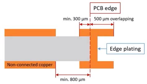
In general, soldermask and silkscreen should be kept away from the plated edges of the PCB to avoid interfering with the connection between the edges and other components. A minimum clearance of 0.5-1.0 mm is typically recommended.
Panelization
Panelization is the process of arranging multiple PCBs on a single panel for manufacturing purposes. When designing a PCB with edge plating, it is important to consider how the board will be panelized and separated from the panel after plating.
One common method is to use a set of tabs or “mouse bites” along the edges of the PCB that can be easily broken off after plating. Another option is to use a routing or scoring process to separate the individual boards from the panel. In either case, it is important to ensure that the panelization method does not damage or interfere with the plated edges of the PCB.
Electrical and Mechanical Testing
Once the PCB has been designed and manufactured, it is important to perform thorough electrical and mechanical testing to ensure that the edge plating meets the required specifications. Electrical testing may include continuity, resistance, and insulation resistance measurements, while mechanical testing may involve cross-sectioning, peel strength, and thermal cycling.
Any defects or issues identified during testing should be addressed before the PCB is put into production. This may involve adjusting the plating process parameters, modifying the PCB design, or implementing additional quality control measures.

Applications of PCB Edge Plating
PCB edge plating is used in a wide range of applications across various industries, including:
-
Consumer Electronics: Edge plating is commonly used in smartphones, tablets, and other portable devices where space is at a premium. By utilizing the edges of the PCB for connections, designers can create more compact and lightweight devices.
-
Automotive Electronics: In the automotive industry, edge plating is used in a variety of applications, such as engine control modules, infotainment systems, and sensors. The enhanced mechanical strength and vibration resistance provided by edge plating are particularly important in this industry.
-
Medical Devices: Edge plating is used in medical devices such as implantable electronics, diagnostic equipment, and surgical tools. The improved signal integrity and reliability offered by edge plating are critical in these applications, where device failure can have serious consequences.
-
Aerospace and Defense: In the aerospace and defense industries, edge plating is used in applications such as avionics, satellite communications, and military electronics. The space savings and enhanced mechanical strength provided by edge plating are essential in these applications, where size and weight are critical factors.
-
Industrial Automation: Edge plating is used in various industrial automation applications, such as process control systems, robotics, and machine vision. The improved connectivity and signal integrity offered by edge plating help ensure reliable operation in harsh industrial environments.
Frequently Asked Questions (FAQ)
-
What is the difference between electroless and electrolytic plating?
Electroless plating is a chemical process that deposits a layer of metal on a surface without the use of an external electrical current. Electrolytic plating, also known as electroplating, uses an electrical current to deposit metal ions onto a conductive surface. Electroless plating is typically used for non-conductive surfaces or hard-to-reach areas, while electroplating is used for conductive surfaces and can achieve thicker deposits. -
Can PCB edge plating be used with other metals besides copper?
Yes, PCB edge plating can be performed with other metals, such as nickel, gold, and silver. These metals are often used as finish layers over the copper plating to improve solderability, corrosion resistance, or electrical conductivity. However, copper is the most common base layer for edge plating due to its excellent electrical and mechanical properties. -
How does PCB edge plating compare to other methods of connecting PCB layers, such as vias or through-hole components?
PCB edge plating offers several advantages over other methods of connecting PCB layers. Compared to vias, edge plating provides a larger surface area for connections, which can improve signal integrity and power handling. Compared to through-hole components, edge plating eliminates the need for additional drilling and assembly steps, which can reduce manufacturing costs and improve reliability. -
What are the typical dimensions for PCB edge plating?
The typical dimensions for PCB edge plating depend on the specific application and design requirements. However, some general guidelines include: - Hole diameter: 0.5-1.0 mm
- Hole spacing: 1.5-2.0 times the hole diameter
- Copper thickness: 25-50 μm
-
Soldermask and silkscreen clearance: 0.5-1.0 mm
-
What are the environmental and safety considerations for PCB edge plating?
PCB edge plating involves the use of chemicals that can be hazardous to human health and the environment if not handled properly. Some key considerations include: - Proper ventilation and personal protective equipment (PPE) should be used when working with plating chemicals.
- Waste materials, such as spent plating solutions and rinse water, must be disposed of in accordance with local and national regulations.
- Regular monitoring and maintenance of plating equipment and solutions are necessary to ensure safe and efficient operation.
- Employees should receive proper training on the safe handling and use of plating chemicals and equipment.
Conclusion
PCB edge plating is a valuable technique for creating electrical connections between the layers of a PCB while saving space and improving signal integrity. By depositing a layer of copper on the edges of the board using an electroless plating process, designers can create more compact, reliable, and cost-effective electronic devices.
When designing a PCB with edge plating, it is important to consider factors such as hole size and spacing, copper thickness, soldermask and silkscreen placement, and panelization. Proper electrical and mechanical testing is also essential to ensure that the plated edges meet the required specifications.
PCB edge plating is used in a wide range of applications, from consumer electronics and automotive systems to medical devices and aerospace equipment. As electronic devices continue to become smaller and more complex, the importance of PCB edge plating will only continue to grow.
By understanding the principles, processes, and applications of PCB edge plating, designers and manufacturers can create innovative and high-performance electronic products that meet the demands of today’s fast-paced and constantly evolving market.
No responses yet