Introduction
Printed Circuit Boards (PCBs) are the backbone of modern electronics. They provide a platform for components to be mounted and connected, allowing for complex circuits to be created in a compact and efficient manner. One of the critical aspects of PCB manufacturing is drilling holes for component leads, vias, and mounting points. The size of these holes, known as PCB drill sizes, plays a crucial role in the functionality and reliability of the final product. In this article, we will dive deep into the world of PCB drill sizes, exploring their importance, standard sizes, and best practices for selecting the right drill size for your project.
The Importance of PCB Drill Sizes
Component Compatibility
PCB drill sizes are essential for ensuring that components can be properly mounted on the board. Each component has specific lead sizes that must be accommodated by the corresponding drill holes. If the holes are too small, the component leads may not fit, making it impossible to solder them in place. On the other hand, if the holes are too large, the components may not be held securely, leading to potential failures or short circuits.
Manufacturing Feasibility
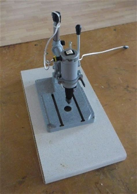
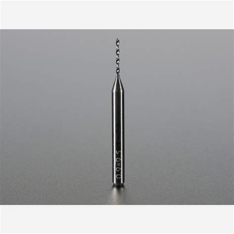
The choice of PCB drill sizes also impacts the manufacturing process. Smaller drill sizes require more precise and expensive equipment, increasing the overall cost of production. Additionally, smaller drill bits are more prone to breakage, which can lead to delays and increased manufacturing time. It is essential to strike a balance between the required precision and the feasibility of manufacturing when selecting PCB drill sizes.
Signal Integrity
In high-speed and high-frequency PCB designs, the size of the drill holes can impact signal integrity. Larger holes can create discontinuities in the signal path, leading to reflections and impedance mismatches. These issues can cause signal degradation, crosstalk, and other unwanted effects. By carefully selecting the appropriate drill sizes and utilizing techniques such as via stitching and controlled impedance drilling, designers can minimize these signal integrity challenges.
Standard PCB Drill Sizes
Imperial Units
In the United States and other countries using imperial units, PCB drill sizes are typically expressed in inches. Some common imperial drill sizes include:
| Drill Size (inches) | Application |
|---|---|
| 0.0135″ | Small component leads, vias |
| 0.0160″ | General-purpose component leads |
| 0.0240″ | Larger component leads, connector pins |
| 0.0320″ | Mounting holes, large connector pins |
| 0.0400″ | Mounting holes, power connectors |
Metric Units
In countries using metric units, PCB drill sizes are expressed in millimeters. Some common metric drill sizes include:
| Drill Size (mm) | Application |
|---|---|
| 0.3mm | Small component leads, vias |
| 0.4mm | General-purpose component leads |
| 0.6mm | Larger component leads, connector pins |
| 0.8mm | Mounting holes, large connector pins |
| 1.0mm | Mounting holes, power connectors |
Drill Size Increments
PCB drill sizes are available in standard increments to accommodate a wide range of components and applications. These increments can vary depending on the manufacturer and the specific requirements of the project. Some common drill size increments include:
- 0.1mm (for metric sizes)
- 0.05mm (for metric sizes requiring higher precision)
- 0.001″ (for imperial sizes)
- 0.0005″ (for imperial sizes requiring higher precision)

Selecting the Right PCB Drill Size
Component Requirements
The primary factor in selecting the appropriate PCB drill size is the component requirements. Each component has specific lead sizes that must be accommodated by the corresponding drill holes. Designers should refer to the component datasheets and application notes to determine the recommended drill sizes for each component.
PCB Thickness
The thickness of the PCB also plays a role in determining the appropriate drill sizes. Thicker PCBs may require larger drill sizes to ensure proper plating and hole wall coverage. The aspect ratio, which is the ratio of the hole depth to the hole diameter, should be considered when selecting drill sizes for thick PCBs. A general rule of thumb is to maintain an aspect ratio of 10:1 or less to ensure reliable plating and hole quality.
Manufacturing Capabilities
The manufacturing capabilities of the PCB fabricator should also be taken into account when selecting drill sizes. Some manufacturers may have limitations on the minimum drill size they can accommodate or the precision they can achieve. It is essential to communicate with the fabricator early in the design process to ensure that the selected drill sizes are compatible with their manufacturing capabilities.
Cost Considerations
As mentioned earlier, smaller drill sizes require more precise and expensive manufacturing equipment, which can increase the overall cost of the PCB. Designers should consider the cost implications of their drill size choices and strike a balance between the required precision and the budget constraints of the project. In some cases, it may be more cost-effective to use larger drill sizes and adjust the component selection accordingly.
Best Practices for PCB Drill Sizes
Standardization
Whenever possible, designers should strive to use standard drill sizes in their PCB designs. Standardization helps to simplify the manufacturing process, reduce the risk of errors, and minimize the cost of production. By using a limited set of standard drill sizes, designers can also optimize the use of drill bits and reduce the need for tool changes during manufacturing.
Hole Tolerance
It is important to specify the appropriate hole tolerances for each drill size used in the PCB design. The hole tolerance defines the acceptable range of variation in the hole diameter. Tighter tolerances require more precise manufacturing processes and may increase the cost of production. Designers should work with the PCB fabricator to determine the appropriate hole tolerances based on the specific requirements of the project.
Plated vs. Non-Plated Holes
PCB holes can be either plated or non-plated, depending on their intended purpose. Plated holes are used for component leads and vias, as they provide an electrical connection between layers of the PCB. Non-plated holes are used for mounting points and other mechanical purposes. Designers should clearly specify which holes require plating and which do not to avoid confusion and ensure the proper manufacturing of the PCB.
Pad Size and Annular Ring
The pad size and annular ring around each hole are critical factors in ensuring the reliability and manufacturability of the PCB. The pad size should be large enough to accommodate the component lead and provide sufficient area for soldering. The annular ring, which is the copper area around the hole, should be wide enough to ensure adequate adhesion between the hole plating and the copper layer. Designers should follow the recommended pad sizes and annular ring widths provided by the PCB fabricator and component manufacturers.
FAQ
1. What is the minimum drill size that can be achieved in PCB manufacturing?
The minimum drill size that can be achieved in PCB manufacturing depends on the capabilities of the specific fabricator. Some advanced fabricators can achieve drill sizes as small as 0.1mm (0.004″) or even smaller. However, it is important to discuss the specific requirements with the fabricator to ensure that they can accommodate the desired drill sizes.
2. Can I use different drill sizes for the same component on a PCB?
In general, it is recommended to use the same drill size for all instances of a particular component on a PCB. Using different drill sizes for the same component can lead to inconsistencies in the manufacturing process and may cause issues with component fit and reliability. If different drill sizes are necessary, it should be clearly communicated to the fabricator, and the potential implications should be carefully considered.
3. How do I ensure that the drill sizes in my PCB design are compatible with the fabricator’s capabilities?
The best way to ensure compatibility between your PCB design and the fabricator’s capabilities is to communicate with the fabricator early in the design process. Provide them with the details of your design, including the desired drill sizes, and ask for their feedback and recommendations. Many fabricators also provide design guidelines and specifications that outline their capabilities and requirements, which can be used as a reference during the design phase.
4. What are the consequences of using drill sizes that are too small or too large?
Using drill sizes that are too small can lead to manufacturing challenges, such as difficulty in plating the holes uniformly or increased risk of drill bit breakage. It can also cause issues with component fit and solderability. On the other hand, using drill sizes that are too large can result in wasted space on the PCB, increased manufacturing costs, and potential signal integrity issues. It is important to strike a balance and choose drill sizes that are appropriate for the specific components and design requirements.
5. Can I use non-standard drill sizes in my PCB design?
While it is possible to use non-standard drill sizes in a PCB design, it is generally not recommended. Non-standard drill sizes may require custom drill bits and specialized manufacturing processes, which can increase the cost and lead time of the project. Additionally, using non-standard sizes can limit the options for component selection and may make it more difficult to find compatible parts in the future. If non-standard drill sizes are necessary, it is important to discuss the requirements with the fabricator and ensure that they can accommodate the specific sizes needed.
Conclusion
PCB drill sizes are a critical aspect of PCB design and manufacturing. They impact component compatibility, manufacturing feasibility, signal integrity, and overall cost. By understanding the standard drill sizes, selecting the appropriate sizes for each component, and following best practices for hole tolerance, plating, and pad design, designers can create PCBs that are reliable, manufacturable, and cost-effective.
When designing a PCB, it is essential to consider the specific requirements of the project, the capabilities of the fabricator, and the potential trade-offs between precision and cost. By working closely with the fabricator and adhering to industry standards and guidelines, designers can ensure that their PCB designs are optimized for performance, reliability, and manufacturability.
As PCB technology continues to evolve, the importance of selecting the right drill sizes will only continue to grow. By staying up-to-date with the latest advancements in PCB manufacturing and design techniques, engineers and designers can create PCBs that push the boundaries of performance and functionality while maintaining the highest standards of quality and reliability.
No responses yet