Introduction to PCB Design
Printed Circuit Board (PCB) design is a crucial aspect of electronic product development. It involves creating a layout for the electrical components and their interconnections on a PCB. A well-designed PCB ensures the proper functioning, reliability, and manufacturability of the electronic device. In this comprehensive tutorial, we will delve into the fundamentals of PCB design and provide you with the knowledge and tools necessary to create high-quality PCBs.
Understanding the Basics of PCB Design
What is a PCB?
A PCB is a flat, insulating board that serves as a base for mounting and interconnecting electronic components. It consists of conductive tracks, pads, and other features etched from copper sheets laminated onto a non-conductive substrate. PCBs are used in virtually all electronic devices, from simple gadgets to complex industrial systems.
Types of PCBs
PCBs can be classified into different types based on their construction and complexity:
- Single-sided PCBs: These PCBs have components and conductive tracks on only one side of the board.
- Double-sided PCBs: These PCBs have components and conductive tracks on both sides of the board, with through-hole connections called vias.
- Multi-layer PCBs: These PCBs consist of multiple layers of conductive tracks separated by insulating layers, allowing for higher component density and more complex designs.
- Flexible PCBs: These PCBs are made from flexible materials, allowing them to bend and conform to various shapes.
- Rigid-Flex PCBs: These PCBs combine rigid and flexible sections, providing both stability and flexibility where needed.
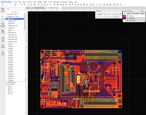
PCB Design Software
To create PCB designs, you will need specialized software tools. Some popular PCB design software options include:
- Altium Designer
- OrCAD
- Eagle
- KiCad
- Autodesk EAGLE
These software tools provide a range of features and capabilities for schematic capture, layout design, and manufacturing output generation.
PCB Design Workflow
Schematic Capture
The first step in PCB design is creating a schematic diagram that represents the electronic circuit. The schematic captures the components, their values, and the connections between them. It serves as a blueprint for the PCB layout.
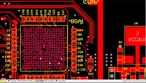
Component Selection and Placement
Once the schematic is complete, the next step is to select the physical components that will be used on the PCB. Consider factors such as package size, power dissipation, and availability when choosing components. Place the components strategically on the board, keeping in mind factors like signal integrity, thermal management, and mechanical constraints.
Routing and Trace Design
After component placement, the next step is to route the traces that connect the components. Traces are the conductive paths that carry electrical signals between components. Consider the following when designing traces:
- Trace width: Determine the appropriate trace width based on the current carrying capacity and signal integrity requirements.
- Trace spacing: Ensure adequate spacing between traces to minimize crosstalk and interference.
- Trace routing: Route traces efficiently to minimize board size and signal path length. Avoid sharp angles and use smooth curves for better signal integrity.
Power and Ground Planes
Proper power distribution is essential for the reliable operation of the PCB. Create power and ground planes to provide low-impedance power distribution and minimize noise. Use appropriate decoupling capacitors near power-hungry components to stabilize the power supply.
Signal Integrity and EMC Considerations
Signal integrity and electromagnetic compatibility (EMC) are critical aspects of PCB design. Consider the following:
- Impedance matching: Match the impedance of traces to the source and load impedances to minimize reflections and signal distortion.
- Crosstalk mitigation: Minimize crosstalk between adjacent traces by using appropriate spacing, shielding, or guard traces.
- EMI reduction: Implement techniques like proper grounding, shielding, and filtering to reduce electromagnetic interference (EMI).
Design Rule Checking (DRC)
Before finalizing the PCB layout, perform design rule checking (DRC) to ensure that the design adheres to the manufacturing constraints and guidelines. DRC checks for issues like minimum trace width, clearance, and drill sizes. Resolve any DRC violations to ensure manufacturability.
Manufacturing Output Generation
Once the PCB design is complete and has passed DRC, generate the necessary manufacturing output files. These typically include:
- Gerber files: These are the industry-standard files that represent the PCB layers, drill holes, and other features.
- Drill files: These files specify the locations and sizes of the drill holes on the PCB.
- Bill of Materials (BOM): This is a list of all the components used on the PCB, including their quantities, part numbers, and specifications.

Advanced PCB Design Techniques
High-Speed Design Considerations
When designing PCBs for high-speed applications, additional considerations come into play:
- Controlled impedance: Use controlled impedance techniques to maintain signal integrity at high frequencies.
- Differential signaling: Employ differential signaling for high-speed data transmission to reduce noise and improve signal quality.
- Length matching: Match the lengths of critical signal traces to minimize skew and ensure proper timing.
Thermal Management
Proper thermal management is crucial for PCBs with high-power components or high-density designs:
- Thermal vias: Use thermal vias to dissipate heat from components to the PCB’s copper layers or heatsinks.
- Copper pours: Use large copper pours on the PCB to spread heat and improve thermal dissipation.
- Heatsinks: Incorporate heatsinks for components that generate significant heat to prevent overheating and ensure reliable operation.
Manufacturability and Assembly Considerations
Consider the following aspects to ensure the manufacturability and ease of assembly of your PCB:
- Component footprints: Use accurate and standard component footprints to ensure proper fitment during assembly.
- Solder mask and silkscreen: Apply solder mask to protect the PCB from short circuits and use silkscreen to label components and provide assembly instructions.
- Panelization: If producing multiple PCBs, consider panelizing the design to optimize manufacturing efficiency.
PCB Design Best Practices
Schematic Organization and Documentation
- Use hierarchical schematic design to break down complex circuits into manageable blocks.
- Provide clear and concise documentation, including component values, reference designators, and net names.
Component Placement and Orientation
- Place components logically and group them based on functionality to simplify routing and minimize signal path lengths.
- Orient components consistently to facilitate assembly and troubleshooting.
Trace Routing and Optimization
- Route traces on appropriate layers based on their signal characteristics and requirements.
- Minimize trace lengths and avoid unnecessary crossings to reduce parasitic effects and improve signal integrity.
- Use via stitching and copper pours to create low-impedance return paths and minimize loop areas.
Grounding and Shielding
- Implement a solid grounding scheme to provide a low-impedance return path for signals.
- Use ground planes and grounding vias to create a stable reference for signals.
- Employ shielding techniques, such as grounded guard traces or shielding cans, to reduce EMI and crosstalk.
Design for Testability and Debugging
- Provide test points and probe pads for critical signals to facilitate testing and debugging.
- Include debugging features, such as JTAG or SWD interfaces, for programming and debugging microcontrollers.
Common PCB Design Mistakes to Avoid
- Insufficient clearance between components and traces, leading to short circuits or manufacturing issues.
- Incorrect component footprints or orientation, causing assembly problems.
- Inadequate power distribution and decoupling, resulting in noise and signal integrity issues.
- Neglecting signal integrity and EMC considerations, leading to performance degradation or compliance failures.
- Overlooking thermal management requirements, causing overheating and reliability problems.
PCB Design Resources and References
- IPC (Association Connecting Electronics Industries) standards: A set of industry-recognized standards for PCB design and manufacturing.
- PCB design forums and communities: Online platforms where PCB designers can seek advice, share knowledge, and collaborate with peers.
- Component manufacturer datasheets and application notes: Valuable resources for selecting and using components effectively in PCB designs.
- PCB fabrication and assembly services: Companies that specialize in manufacturing and assembling PCBs based on design files.
Frequently Asked Questions (FAQ)
- What is the difference between a schematic and a PCB layout?
-
A schematic is a graphical representation of the electrical connections and components in a circuit, while a PCB layout is the physical arrangement of those components and the conductive tracks that connect them on a PCB.
-
How do I choose the appropriate trace width for my PCB design?
-
The appropriate trace width depends on factors such as the current carrying capacity, signal integrity requirements, and the manufacturing capabilities of the PCB fabricator. Refer to IPC-2221 standards and consult with your fabricator for guidance on trace width selection.
-
What is the purpose of a solder mask on a PCB?
-
A solder mask is a protective coating applied to the copper traces on a PCB. It serves to prevent short circuits, protect the traces from oxidation and contamination, and provide electrical insulation. The solder mask also helps to define the areas where solder should be applied during the assembly process.
-
How can I minimize crosstalk between traces on a PCB?
-
To minimize crosstalk, consider the following techniques:
- Increase the spacing between adjacent traces.
- Route sensitive traces on different layers or use guard traces.
- Use differential signaling for high-speed signals.
- Minimize parallel run lengths of traces that may couple.
- Employ proper grounding and shielding techniques.
-
What are the benefits of using a multi-layer PCB instead of a single-layer or double-layer PCB?
- Multi-layer PCBs offer several benefits:
- Increased component density and routing possibilities.
- Improved signal integrity due to dedicated power and ground planes.
- Better EMI performance through the use of shielding layers.
- Enhanced thermal dissipation with the use of internal copper layers.
- Reduced board size and weight compared to single-layer or double-layer PCBs with the same functionality.
Conclusion
PCB design is a critical skill for anyone involved in electronic product development. By understanding the fundamentals of PCB design, following best practices, and utilizing the right tools and resources, you can create high-quality PCBs that meet your project requirements. Remember to consider factors such as signal integrity, power distribution, thermal management, and manufacturability throughout the design process.
As you gain experience and tackle more complex designs, continue to learn and stay updated with the latest techniques and technologies in PCB design. Collaborate with experienced designers, participate in online communities, and refer to industry standards and guidelines to further enhance your skills.
With practice and perseverance, you can become proficient in PCB design and contribute to the development of innovative electronic products. Happy designing!
No responses yet