Introduction to Optocouplers and Their Role in PCB Design
Optocouplers, also known as optoisolators or photocouplers, are essential components in PCB design that provide electrical isolation between different parts of a circuit. They play a crucial role in protecting sensitive components, improving signal integrity, and ensuring the overall reliability of the PCB. In this comprehensive tutorial, we will dive into the world of optocouplers and explore tips and best practices for effectively incorporating them into your PCB layout.
Understanding the Basics of Optocouplers
What is an Optocoupler?
An optocoupler is an electronic component that uses light to transmit electrical signals between two isolated circuits. It consists of an LED (light-emitting diode) and a phototransistor or photodiode encased in a single package. The LED converts the electrical signal into light, which is then detected by the phototransistor or photodiode, converting it back into an electrical signal.
Key Benefits of Using Optocouplers in PCB Design
- Electrical Isolation: Optocouplers provide galvanic isolation between different parts of a circuit, preventing ground loops, noise, and interference.
- Protection: They protect sensitive components from voltage spikes, transients, and other electrical disturbances.
- Signal Integrity: Optocouplers help maintain signal integrity by eliminating ground loops and reducing electromagnetic interference (EMI).
- Flexibility: They allow for the integration of circuits with different voltage levels or ground references.
Selecting the Right Optocoupler for Your PCB
Types of Optocouplers
There are several types of optocouplers available, each with its own characteristics and applications. Some common types include:
- Phototransistor Optocouplers: These optocouplers use a phototransistor as the output device, providing high current transfer ratios and fast switching speeds.
- Photodiode Optocouplers: These optocouplers use a photodiode as the output device, offering high linearity and low distortion.
- MOSFET Optocouplers: These optocouplers incorporate a MOSFET (metal-oxide-semiconductor field-effect transistor) as the output device, providing high isolation voltage and fast switching speeds.
Key Specifications to Consider
When selecting an optocoupler for your PCB, consider the following key specifications:
- Current Transfer Ratio (CTR): The ratio of the output current to the input current. Higher CTR values indicate better efficiency.
- Isolation Voltage: The maximum voltage that can be applied between the input and output circuits without causing breakdown.
- Switching Speed: The time required for the optocoupler to switch from one state to another. Faster switching speeds are desirable for high-speed applications.
- Package Type: Optocouplers come in various package types, such as DIP (dual in-line package), SMD (surface-mount device), and THT (through-hole technology). Choose the package type that suits your PCB design and manufacturing process.

PCB Layout Considerations for Optocouplers
Placement and Orientation
When placing optocouplers on your PCB, consider the following guidelines:
- Keep the input and output circuits on opposite sides of the optocoupler to maximize isolation.
- Orient the optocoupler so that the LED and phototransistor/photodiode are aligned for optimal light transmission.
- Avoid placing optocouplers near high-frequency or high-current traces to minimize interference.
Trace Routing and Clearance
Proper trace routing and clearance are essential for maintaining signal integrity and isolation. Follow these tips:
- Route the input and output traces away from each other to minimize crosstalk.
- Maintain sufficient clearance between the optocoupler pins and other components to avoid short circuits.
- Use guard rings or ground planes around the optocoupler to provide additional shielding and reduce EMI.
Power Supply Decoupling
Decoupling the power supply is crucial for stable operation of optocouplers. Consider the following practices:
- Place decoupling capacitors close to the optocoupler’s power pins to minimize noise and transients.
- Use separate power supplies for the input and output circuits to ensure proper isolation.
- Implement appropriate filtering and regulation techniques to provide clean and stable power to the optocoupler.
Optocoupler Power Dissipation and Thermal Management
Optocouplers generate heat during operation, which can affect their performance and reliability. To manage power dissipation and thermal issues:
- Select optocouplers with appropriate power ratings for your application.
- Use heatsinks or thermal pads to dissipate heat away from the optocoupler.
- Provide sufficient copper area around the optocoupler pins for effective heat dissipation.
- Consider the ambient temperature and ventilation requirements of your PCB enclosure.
Optocoupler PCB Design Examples
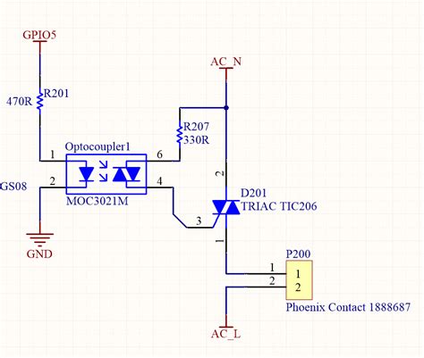
Example 1: Isolated Digital Input
In this example, we will design a PCB layout for an isolated digital input using an optocoupler.
- Select a suitable optocoupler, such as the TLP181, which is a phototransistor optocoupler with a high CTR and fast switching speed.
- Place the optocoupler on the PCB, keeping the input and output circuits on opposite sides.
- Route the input signal trace to the LED anode and connect the LED cathode to ground through a current-limiting resistor.
- Route the output signal trace from the phototransistor collector to the next stage of the circuit.
- Connect the phototransistor emitter to ground.
- Place decoupling capacitors close to the optocoupler’s power pins.
- Use guard rings or ground planes around the optocoupler for additional shielding.
Example 2: Isolated Analog Signal Transmission
In this example, we will design a PCB layout for transmitting an isolated analog signal using an optocoupler.
- Select a suitable optocoupler, such as the HCNR200, which is a high-linearity analog optocoupler.
- Place the optocoupler on the PCB, keeping the input and output circuits on opposite sides.
- Route the input analog signal trace to the LED anode and connect the LED cathode to a constant current source.
- Route the output signal trace from the photodiode cathode to the next stage of the circuit.
- Connect the photodiode anode to a stable reference voltage.
- Implement appropriate filtering and amplification stages for the output analog signal.
- Use guard rings or ground planes around the optocoupler for additional shielding.
Common Mistakes to Avoid in Optocoupler PCB Design
- Inadequate Isolation: Failing to provide sufficient isolation between the input and output circuits can compromise the effectiveness of the optocoupler.
- Incorrect Placement: Placing optocouplers too close to high-frequency or high-current traces can lead to interference and signal degradation.
- Improper Power Supply Decoupling: Neglecting to properly decouple the power supply can introduce noise and transients, affecting the optocoupler’s performance.
- Insufficient Heat Dissipation: Overlooking thermal management considerations can lead to overheating and reduced reliability of the optocoupler.
- Inadequate Trace Clearance: Failing to maintain sufficient clearance between the optocoupler pins and other components can result in short circuits and signal integrity issues.
Frequently Asked Questions (FAQ)
-
Q: What is the difference between an optocoupler and a relay?
A: An optocoupler uses light to transmit signals between isolated circuits, while a relay uses an electromagnetic coil to mechanically switch contacts. Optocouplers provide faster switching speeds and longer lifetimes compared to relays. -
Q: Can optocouplers be used for both digital and analog signals?
A: Yes, optocouplers can be used for both digital and analog signals. Phototransistor optocouplers are commonly used for digital signals, while photodiode optocouplers are suitable for analog signals. -
Q: How do I select the appropriate current-limiting resistor for the LED in an optocoupler?
A: The current-limiting resistor value depends on the LED’s forward voltage and the desired forward current. Consult the optocoupler’s datasheet for recommended values and use Ohm’s law to calculate the resistor value. -
Q: Can optocouplers protect against high-voltage transients?
A: Yes, optocouplers provide isolation and protection against high-voltage transients. However, ensure that the optocoupler’s isolation voltage rating is sufficient for your application’s requirements. -
Q: How can I minimize crosstalk between optocoupler channels in multi-channel designs?
A: To minimize crosstalk, use separate ground planes or guard rings for each optocoupler channel, route the input and output traces away from each other, and provide sufficient spacing between channels.
Conclusion
Optocouplers are valuable components in PCB design, offering electrical isolation, protection, and signal integrity benefits. By understanding the basics of optocouplers, selecting the right type for your application, and following best practices for PCB layout, you can effectively incorporate optocouplers into your designs.
Remember to consider factors such as placement, trace routing, power supply decoupling, and thermal management when designing with optocouplers. Avoid common mistakes and refer to the examples and guidelines provided in this tutorial to ensure optimal performance and reliability.
By mastering the use of optocouplers in your PCB layouts, you can create robust and reliable designs that meet the demands of various applications. Happy designing!
No responses yet