Introduction
Printed Circuit Board (PCB) design is a crucial aspect of electronic product development. It involves creating a board that connects various electronic components to form a functional circuit. PCB design requires a team of skilled professionals working together to ensure the final product meets the desired specifications and performs optimally. In this article, we will explore the roles and responsibilities of the PCB design team and how they collaborate to create high-quality PCBs.
The Importance of a Well-Structured PCB Design Team
A well-structured PCB design team is essential for the success of any electronic product development project. The team should consist of individuals with diverse skill sets and expertise, working together to achieve a common goal. Each team member has specific responsibilities and contributes to the overall success of the project.
Benefits of a Well-Structured PCB Design Team
- Improved efficiency and productivity
- Better communication and collaboration
- Faster problem-solving and decision-making
- Increased innovation and creativity
- Higher quality products and reduced errors
Key Roles in a PCB Design Team
1. PCB Designer
The PCB designer is responsible for creating the physical layout of the PCB. They use specialized software to place components, route traces, and ensure that the board meets all the necessary design requirements. The PCB designer works closely with other team members to optimize the layout for manufacturability, reliability, and performance.
Responsibilities of a PCB Designer
- Creating schematic diagrams and board layouts
- Selecting appropriate components and materials
- Ensuring design compliance with industry standards and regulations
- Collaborating with other team members to optimize the design
- Generating manufacturing files and documentation
2. Electrical Engineer
The electrical engineer is responsible for designing the electrical circuit that will be implemented on the PCB. They work closely with the PCB designer to ensure that the circuit is properly laid out on the board and that all components are connected correctly. The electrical engineer also performs simulations and tests to verify the circuit’s functionality and performance.
Responsibilities of an Electrical Engineer
- Designing the electrical circuit schematic
- Selecting appropriate components and defining their specifications
- Performing circuit simulations and analyses
- Collaborating with the PCB designer to optimize the layout
- Testing and validating the final circuit design
3. Mechanical Engineer
The mechanical engineer is responsible for designing the physical enclosure and mounting hardware for the PCB. They ensure that the board fits properly within the enclosure and that it is protected from environmental factors such as heat, vibration, and moisture. The mechanical engineer also considers factors such as manufacturability, assembly, and maintainability when designing the enclosure.
Responsibilities of a Mechanical Engineer
- Designing the enclosure and mounting hardware
- Ensuring proper fit and protection for the PCB
- Optimizing the design for manufacturability and assembly
- Collaborating with the PCB designer and electrical engineer to ensure compatibility
- Creating 3D models and detailed drawings of the enclosure
4. Test Engineer
The test engineer is responsible for developing and executing test plans to verify the functionality, reliability, and performance of the PCB. They work closely with the electrical engineer to identify potential issues and ensure that the board meets all the necessary requirements. The test engineer also develops test fixtures and jigs to facilitate the testing process.
Responsibilities of a Test Engineer
- Developing comprehensive test plans and procedures
- Designing and building test fixtures and jigs
- Executing tests and analyzing results
- Identifying and reporting issues or defects
- Collaborating with other team members to resolve problems and improve the design
5. Project Manager
The project manager is responsible for overseeing the entire PCB design project from start to finish. They coordinate the efforts of all team members, ensure that project goals and deadlines are met, and communicate with stakeholders to keep them informed of progress and any issues that arise. The project manager also manages the project budget and resources to ensure that the project stays on track.
Responsibilities of a Project Manager
- Defining project scope, goals, and deliverables
- Developing and managing project schedules and budgets
- Coordinating and communicating with team members and stakeholders
- Identifying and mitigating project risks and issues
- Ensuring project quality and compliance with standards and regulations

Collaboration and Communication in PCB Design Teams
Effective collaboration and communication are essential for the success of any PCB design project. Team members must work together closely to ensure that all aspects of the design are properly integrated and optimized. Regular meetings, design reviews, and status updates help keep everyone informed and on the same page.
Best Practices for Collaboration and Communication
- Establish clear roles and responsibilities for each team member
- Use a centralized project management tool to track progress and share information
- Conduct regular design reviews to identify and address issues early in the process
- Encourage open and honest communication among team members
- Foster a culture of continuous improvement and learning
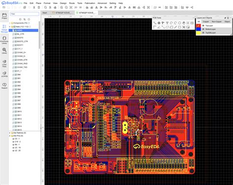
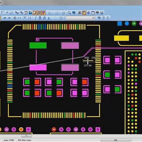
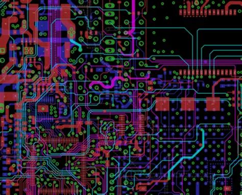
Tools and Technologies for PCB Design Teams
PCB design teams rely on a variety of tools and technologies to create high-quality boards efficiently and effectively. These tools include:
| Tool Category | Examples |
|---|---|
| PCB Design Software | Altium Designer, OrCAD, Eagle, KiCad |
| Schematic Capture Software | Altium Designer, OrCAD Capture, Eagle, KiCad |
| Simulation and Analysis Tools | SPICE, HyperLynx, Ansys SIwave |
| Collaboration and Project Management Tools | Altium 365, GitHub, Jira, Trello |
| Testing and Measurement Equipment | Oscilloscopes, Multimeters, Spectrum Analyzers, Logic Analyzers |
Frequently Asked Questions (FAQ)
1. What skills are required to become a PCB designer?
To become a PCB designer, one should have a strong understanding of electronic circuits, component specifications, and PCB manufacturing processes. Proficiency in PCB design software, such as Altium Designer or OrCAD, is also essential. Good problem-solving skills, attention to detail, and the ability to work well in a team are important soft skills for a PCB designer.
2. How do PCB design teams ensure that the final product meets all the necessary requirements?
PCB design teams use a combination of design reviews, simulations, and testing to ensure that the final product meets all the necessary requirements. Regular design reviews help identify and address issues early in the process, while simulations and analyses verify the circuit’s functionality and performance. Comprehensive testing and validation of the final product ensure that it meets all the specified requirements and performs as expected.
3. What are some common challenges faced by PCB design teams, and how can they be overcome?
Some common challenges faced by PCB design teams include managing complex designs, ensuring compatibility between different components and subsystems, and meeting tight deadlines and budgets. These challenges can be overcome by fostering effective communication and collaboration among team members, using appropriate tools and technologies, and implementing best practices for project management and quality control.
4. How important is documentation in the PCB design process?
Documentation is crucial in the PCB design process, as it ensures that all team members have access to the necessary information and can refer to it throughout the project. Proper documentation also facilitates communication with stakeholders, such as manufacturers and clients, and helps maintain a record of the design decisions and changes made during the project. Maintaining accurate and up-to-date documentation can help streamline the design process and reduce errors and rework.
5. What steps can PCB design teams take to continuously improve their processes and products?
PCB design teams can continuously improve their processes and products by regularly reviewing their performance, identifying areas for improvement, and implementing changes based on lessons learned. Conducting post-project reviews, seeking feedback from stakeholders, and staying up-to-date with the latest industry trends and best practices can help teams identify opportunities for improvement. Encouraging a culture of continuous learning and innovation within the team can also contribute to ongoing process and product enhancements.
Conclusion
In conclusion, a well-structured and collaborative PCB design team is essential for the success of any electronic product development project. By understanding the roles and responsibilities of each team member, fostering effective communication and collaboration, and utilizing appropriate tools and technologies, PCB design teams can create high-quality boards that meet all the necessary requirements and perform optimally. As the electronics industry continues to evolve, PCB design teams must stay adaptable and continuously improve their processes and products to remain competitive and deliver the best possible results.
No responses yet