Introduction to PCB DFT
Designing printed circuit boards (PCBs) with testability in mind, known as design for test (DFT), is crucial for ensuring the quality, reliability, and manufacturability of electronic products. In part 1 of this series, we explored the fundamentals of PCB DFT, including the importance of incorporating testability features early in the design process, common DFT techniques, and the benefits of implementing DFT. In this second part, we will delve deeper into specific DFT structures, the tests they enable, and best practices for incorporating them into your PCB designs.
Types of PCB DFT Structures
There are several types of DFT structures that can be incorporated into PCB designs to facilitate testing and improve testability. Some of the most common DFT structures include:
1. Test Points
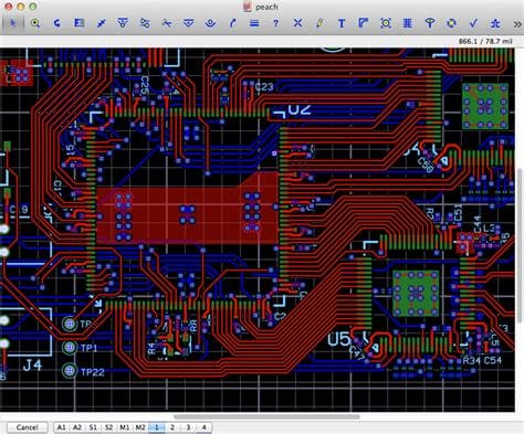
Test points are exposed pads or vias on the PCB that provide access to specific signals or nets for testing purposes. They allow test equipment to probe and measure various parameters, such as voltage levels, signal integrity, and connectivity. Test points can be classified into two main categories:
- Probe Points: These are test points that are accessible from the top or bottom side of the PCB using test probes or needles. They are typically used for manual testing or debugging.
- Boundary Scan Test Points: These test points are specifically designed for boundary scan testing, which is an automated testing technique that uses a special test access port (TAP) to control and observe the state of digital components on the PCB.
2. JTAG/Boundary Scan Chain
JTAG (Joint Test Action Group) is a standard interface and protocol (IEEE 1149.1) used for testing and debugging digital circuits on a PCB. It provides a means to access and control the boundary scan cells of compliant devices, allowing for testing of interconnects, logic functionality, and programming of devices.
A boundary scan chain is formed by connecting the boundary scan cells of multiple devices in a daisy-chain configuration. The chain is accessed through a TAP, which consists of four signals: TDI (Test Data In), TDO (Test Data Out), TMS (Test Mode Select), and TCK (Test Clock).
3. Built-In Self-Test (BIST)
Built-In Self-Test (BIST) is a DFT technique that incorporates self-testing capabilities directly into the digital components on the PCB. BIST structures generate test patterns, apply them to the circuit under test, and compare the output responses with expected results to detect faults.
BIST can be implemented in various forms, such as:
- Memory BIST: Used for testing embedded memories, such as RAM and ROM.
- Logic BIST: Used for testing digital logic circuits, such as processors, ASICs, and FPGAs.
- Analog BIST: Used for testing analog circuits, such as ADCs, DACs, and PLLs.
4. Scan Chain
A scan chain is a DFT structure that allows the internal state of a digital circuit to be controlled and observed externally. It is formed by replacing the regular flip-flops in the circuit with scan flip-flops, which have additional input and output ports for scanning.
During testing, the scan chain is used to shift test patterns into the circuit, capture the output responses, and shift them out for analysis. Scan chains enable efficient testing of complex digital circuits by providing direct access to the internal states.
PCB DFT Tests
With the appropriate DFT structures in place, various tests can be performed on the PCB to verify its functionality, performance, and manufacturing quality. Some of the key tests enabled by DFT include:
1. In-Circuit Testing (ICT)
In-Circuit Testing (ICT) is a test method that verifies the proper assembly and functionality of individual components on the PCB. It involves probing test points on the board using a bed-of-nails fixture and applying test stimuli to check for shorts, opens, resistance, capacitance, and other parameters.
ICT relies on the presence of test points and accessibility to component pins. Proper placement and spacing of test points are critical for successful ICT.
2. Boundary Scan Testing
Boundary scan testing, also known as JTAG testing, is an automated test technique that uses the JTAG interface and boundary scan chain to test interconnects, logic functionality, and programming of boundary scan compliant devices.
The test process involves shifting test patterns into the boundary scan cells, applying them to the circuit under test, capturing the output responses, and comparing them with expected results. Boundary scan testing can detect faults such as opens, shorts, stuck-at faults, and logic errors.
3. Functional Testing
Functional testing verifies that the PCB performs its intended functions and meets the specified requirements. It involves applying test stimuli to the board’s inputs and measuring the outputs to ensure correct behavior.
DFT structures, such as test points and BIST, facilitate functional testing by providing access to critical signals and enabling self-testing capabilities. Functional testing can be performed at various levels, from individual components to the complete system.
4. Flying Probe Testing
Flying probe testing is a non-contact test method that uses movable test probes to access test points on the PCB. The probes can move rapidly across the board, making contact with the test points to perform electrical measurements and functional tests.
Flying probe testing offers flexibility and adaptability, as it does not require a dedicated test fixture. However, it relies on the presence and accessibility of test points on the PCB.

Best Practices for PCB DFT
To effectively implement DFT in your PCB designs, consider the following best practices:
-
Plan for DFT early: Incorporate DFT considerations from the beginning of the design process. This allows for optimal placement of test points, JTAG/boundary scan chain, and other DFT structures.
-
Use standard interfaces: Adhere to industry-standard interfaces, such as JTAG, for boundary scan testing. This ensures compatibility with test equipment and tools.
-
Provide adequate test coverage: Ensure that the DFT structures provide sufficient test coverage for the PCB. Consider the critical signals, components, and interconnects that need to be tested.
-
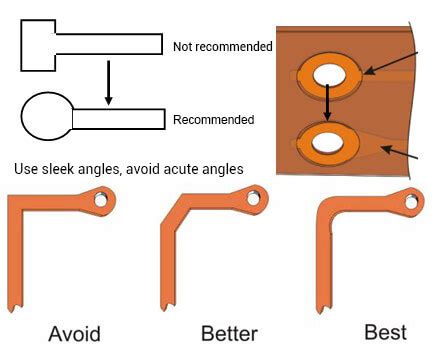
Optimize test point placement: Place test points strategically to minimize the impact on signal integrity and board layout. Follow guidelines for test point size, spacing, and accessibility.
-
Document DFT features: Maintain clear documentation of the DFT structures, test points, and test procedures. This facilitates efficient testing and debugging by the manufacturing and maintenance teams.
-
Collaborate with test engineers: Work closely with test engineers to understand their requirements and ensure that the DFT implementation meets their needs.
-
Verify DFT effectiveness: Perform simulations and prototype testing to validate the effectiveness of the DFT structures and tests. Make necessary adjustments based on the results.
DFT Structures and Tests Table
The following table summarizes the common DFT structures and the tests they enable:
| DFT Structure | Description | Enabled Tests |
|---|---|---|
| Test Points | Exposed pads or vias for probing signals | ICT, Flying Probe Testing |
| JTAG/Boundary Scan | Standard interface for testing and debugging digital circuits | Boundary Scan Testing |
| Built-In Self-Test (BIST) | Self-testing capabilities incorporated into digital components | Functional Testing |
| Scan Chain | Allows control and observation of internal circuit states | Functional Testing |
Frequently Asked Questions (FAQ)
-
Q: What is the difference between ICT and flying probe testing?
A: ICT uses a bed-of-nails fixture to probe test points on the PCB, while flying probe testing uses movable test probes that can access test points without a dedicated fixture. ICT is faster and more suitable for high-volume production, while flying probe testing offers more flexibility and adaptability. -
Q: Can boundary scan testing detect all types of faults on a PCB?
A: Boundary scan testing is effective in detecting faults related to interconnects, logic functionality, and programming of boundary scan compliant devices. However, it may not detect all types of faults, such as analog component failures or faults in non-boundary scan compliant devices. -
Q: How do I determine the optimal number and placement of test points on a PCB?
A: The number and placement of test points depend on factors such as the complexity of the PCB, critical signals, and test coverage requirements. Collaborate with test engineers and follow guidelines for test point size, spacing, and accessibility. Perform simulations and prototype testing to validate the effectiveness of the test point placement. -
Q: What are the benefits of incorporating BIST in PCB designs?
A: BIST provides self-testing capabilities directly within the digital components on the PCB. It enables efficient testing of complex circuits, reduces the need for external test equipment, and can speed up the testing process. BIST also helps diagnose faults at the component level, facilitating localization and repair. -
Q: How does DFT impact the overall cost and time-to-market of a PCB design?
A: Implementing DFT may increase the initial design effort and cost due to the addition of test structures and considerations. However, the long-term benefits of DFT, such as improved testability, reduced manufacturing defects, and faster debugging and repair, often outweigh the initial investments. DFT can ultimately lead to lower overall costs and faster time-to-market by catching and resolving issues early in the development cycle.
Conclusion
PCB design for test (DFT) is a critical aspect of ensuring the quality, reliability, and manufacturability of electronic products. By incorporating appropriate DFT structures, such as test points, JTAG/boundary scan chain, BIST, and scan chain, designers can enable various tests that verify the functionality, performance, and manufacturing quality of the PCB.
Effective implementation of DFT requires careful planning, adherence to best practices, and collaboration with test engineers. By considering DFT early in the design process, optimizing test point placement, and providing adequate test coverage, designers can reap the benefits of improved testability, reduced manufacturing defects, and faster debugging and repair.
As PCB complexity continues to increase and time-to-market pressures intensify, the importance of DFT cannot be overstated. Embracing DFT techniques and structures is essential for delivering high-quality, reliable, and cost-effective electronic products in today’s competitive market.
No responses yet