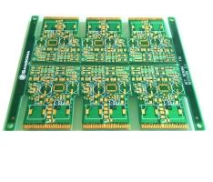
The Importance of Via Design in PCB Manufacturing
Vias play a crucial role in multilayer PCB designs by enabling interconnections between different layers. They allow signals to travel vertically through the board, which is essential for complex designs with limited surface area. However, vias also introduce potential points of failure during the manufacturing process. Some common via defects include:
- Incomplete plating: When the plating inside the via barrel is not uniform or thick enough, it can lead to poor electrical conductivity and intermittent connections.
- Voids: Air bubbles or gaps in the plating can create voids, which weaken the mechanical strength of the via and cause reliability issues.
- Misregistration: If the via holes are not aligned properly with the pads on different layers, it can result in open circuits or poor connections.
To minimize the occurrence of these defects, it’s essential to design vias with manufacturing considerations in mind and maintain open communication with your PCB manufacturer.
Establishing Communication with Your PCB Manufacturer
Before finalizing your PCB design, engage in a dialogue with your chosen manufacturer. Share your design files, including the schematic, layout, and bill of materials (BOM), and discuss any specific requirements or constraints. Some key topics to cover include:
- Manufacturing capabilities: Understand the manufacturer’s equipment, process capabilities, and limitations. This information will help you design vias that are compatible with their production methods.
- Design rules: Request the manufacturer’s design rules and guidelines, which specify parameters such as minimum via size, spacing, and aspect ratio. Adhering to these rules will ensure that your design is manufacturable and less prone to defects.
- Material selection: Discuss the choice of PCB substrate material, as well as the plating options for vias (such as copper, gold, or silver). Different materials have varying electrical and mechanical properties that can affect via reliability.
- Testing and inspection: Inquire about the manufacturer’s quality control processes, including automated optical inspection (AOI), X-ray inspection, and electrical testing. Understanding their testing capabilities will help you design vias that can be easily inspected and verified.
By establishing clear communication channels and expectations with your manufacturer, you can collaborate effectively to create a PCB design that is optimized for manufacturability and reliability.
Best Practices for Via Design
When designing vias for your PCB, consider the following best practices to minimize the risk of defects:
1. Via Size and Aspect Ratio
The size of the via hole and its aspect ratio (the ratio of the via depth to its diameter) are critical factors in ensuring reliable plating and preventing defects. As a general rule, aim for larger via sizes and lower aspect ratios to facilitate better plating coverage and reduce the chances of voids or incomplete plating.
| Via Size (mm) | Aspect Ratio | Plating Challenges |
|---|---|---|
| 0.2 | 8:1 | High |
| 0.3 | 6:1 | Moderate |
| 0.4 | 4:1 | Low |
Table 1: Via size, aspect ratio, and associated plating challenges
Consult with your manufacturer to determine the minimum via size and maximum aspect ratio they can reliably fabricate. In general, it’s recommended to use via sizes of at least 0.3 mm and aspect ratios lower than 6:1 for better manufacturability.
2. Via Spacing and Clearance
Proper spacing between vias and other components, as well as clearance from the board edge, is essential to avoid manufacturing issues. Insufficient spacing can lead to shorting or drilling problems, while inadequate clearance can cause mechanical stress and damage during fabrication.
| Parameter | Minimum Value (mm) |
|---|---|
| Via-to-via spacing | 0.25 |
| Via-to-pad spacing | 0.20 |
| Via-to-board edge clearance | 0.50 |
Table 2: Recommended minimum values for via spacing and clearance
Follow your manufacturer’s design rules for via spacing and clearance, and use the recommended minimum values as a starting point. Increase the spacing and clearance whenever possible to provide more tolerance for manufacturing variations.
3. Via Placement and Routing
The placement of vias on your PCB layout can impact the manufacturing process and the overall reliability of the board. Consider the following guidelines when placing and routing vias:
- Avoid placing vias under components, especially those with high thermal dissipation, as they can interfere with heat transfer and cause soldering issues.
- Place vias in a staggered pattern rather than in a straight line to reduce stress concentration and improve mechanical strength.
- Route traces away from via pads to minimize the risk of shorting or signal integrity issues.
- Use thermal relief pads for vias connected to large copper planes to prevent solder wicking and ensure proper soldering.
By strategically placing vias and routing traces, you can optimize your PCB layout for manufacturability and minimize the occurrence of defects.
4. Via Filling and Capping
In some cases, vias need to be filled or capped to improve the PCB’s mechanical strength, thermal conductivity, or electromagnetic compatibility (EMC). Via filling involves plugging the via barrel with a conductive material, such as copper or silver epoxy, while via capping involves covering the via surface with a conductive layer.
| Method | Purpose | Considerations |
|---|---|---|
| Via filling | – Improve mechanical strength – Enhance thermal conductivity – Provide EMC shielding |
– Increases manufacturing complexity – May require additional processing steps |
| Via capping | – Protect via surface – Improve solderability – Enhance electrical conductivity |
– Requires precise control of the capping process – May impact the PCB’s flatness |
Table 3: Via filling and capping methods, purposes, and considerations
Discuss your via filling or capping requirements with your manufacturer to ensure that they have the capability and expertise to perform these processes reliably. Provide clear instructions on which vias need to be filled or capped, and specify the desired material and process parameters.

Collaborating with Your Manufacturer for Optimal Results
Effective collaboration with your PCB manufacturer is key to preventing via defects and ensuring a successful production run. Throughout the design and manufacturing process, maintain open lines of communication and be receptive to feedback and suggestions from your manufacturer. Some ways to foster a collaborative relationship include:
- Design reviews: Share your PCB design files with the manufacturer and request a design for manufacturability (DFM) review. This review will help identify potential issues, such as via size, spacing, or aspect ratio violations, and provide recommendations for improvement.
- Prototype testing: Before committing to a full production run, consider ordering a small batch of prototypes to validate your design and test the manufacturer’s capabilities. Evaluate the prototypes for via quality, electrical performance, and mechanical integrity, and make any necessary adjustments based on the results.
- Process optimization: Work with your manufacturer to optimize the fabrication process for your specific design requirements. This may involve adjusting plating parameters, drilling speeds, or inspection methods to achieve the best possible via quality and reliability.
- Continuous improvement: Regularly review the manufacturing process and quality metrics with your manufacturer to identify areas for improvement. Collaboratively develop action plans to address any issues or defects, and track progress over time to ensure consistent quality and reliability.
By fostering a strong partnership with your PCB manufacturer and actively collaborating throughout the design and production process, you can minimize the risk of via defects and achieve optimal results for your PCB projects.
Frequently Asked Questions (FAQ)
-
Q: What are the most common causes of via defects in PCB manufacturing?
A: The most common causes of via defects include incomplete plating, voids in the plating, and misregistration between via holes and pads. These issues can arise due to improper via design, incompatible manufacturing processes, or inadequate quality control. -
Q: How can I ensure that my via design is compatible with my manufacturer’s capabilities?
A: To ensure compatibility, request your manufacturer’s design rules and guidelines, which specify parameters such as minimum via size, spacing, and aspect ratio. Adhere to these rules when designing your PCB, and engage in a dialogue with your manufacturer to discuss any specific requirements or constraints. -
Q: What is the recommended minimum via size for reliable manufacturing?
A: As a general guideline, it’s recommended to use via sizes of at least 0.3 mm for better manufacturability. However, the actual minimum via size may vary depending on your manufacturer’s capabilities and the specific requirements of your PCB design. Always consult with your manufacturer to determine the appropriate via size for your project. -
Q: How does via aspect ratio affect the manufacturability of my PCB?
A: The via aspect ratio, which is the ratio of the via depth to its diameter, can impact the plating process and the risk of defects. Higher aspect ratios (greater than 6:1) can lead to plating challenges, such as incomplete coverage or voids. To minimize these risks, aim for lower aspect ratios whenever possible, and discuss the acceptable range with your manufacturer. -
Q: What are the benefits of collaborating closely with my PCB manufacturer throughout the design and production process?
A: Close collaboration with your PCB manufacturer offers several benefits, including: - Identifying and addressing potential design issues early in the process, reducing the risk of defects and delays.
- Optimizing the fabrication process for your specific design requirements, ensuring the best possible quality and reliability.
- Fostering a strong partnership that enables continuous improvement and long-term success for your PCB projects.
By maintaining open communication and actively collaborating with your manufacturer, you can minimize the occurrence of via defects and achieve optimal results for your PCB designs.
Conclusion
Via defects can have a significant impact on the reliability and functionality of a PCB, making it crucial to prioritize via design for manufacturing. By establishing clear communication with your PCB manufacturer, following best practices for via design, and collaborating throughout the production process, you can minimize the risk of defects and ensure the success of your PCB projects.
Remember to:
1. Engage in a dialogue with your manufacturer to understand their capabilities, design rules, and requirements.
2. Design vias with appropriate sizes, aspect ratios, spacing, and clearance to facilitate reliable manufacturing.
3. Consider via placement, routing, filling, and capping options to optimize your PCB layout for manufacturability.
4. Foster a collaborative relationship with your manufacturer through design reviews, prototype testing, process optimization, and continuous improvement.
By implementing these strategies and maintaining a strong focus on via design for manufacturing, you can prevent via defects, improve the quality and reliability of your PCBs, and streamline your production process. Effective communication and collaboration with your PCB manufacturer are key to achieving these goals and ensuring the long-term success of your electronic products.
No responses yet