Introduction to PCB Design
Printed Circuit Board (PCB) design is a crucial aspect of electronic product development. As a new designer, it’s essential to understand the fundamentals of PCB design to create reliable and efficient electronic circuits. In this article, we’ll cover the basics of PCB design, including the design process, important considerations, and best practices.
What is a PCB?
A PCB is a flat board made of insulating material, such as fiberglass or plastic, with conductive copper traces printed on its surface. These traces connect various electronic components, such as resistors, capacitors, and integrated circuits (ICs), to form a complete electronic circuit. PCBs are used in almost all electronic devices, from smartphones and computers to medical equipment and industrial machinery.
Advantages of using PCBs
Using PCBs in electronic product design offers several advantages:
- Compact size: PCBs allow for the miniaturization of electronic circuits, enabling the creation of smaller and more portable devices.
- Reliability: PCBs provide stable and reliable connections between components, reducing the risk of short circuits and other failures.
- Mass production: PCBs are designed for automated assembly, making it easy to mass-produce electronic devices at a lower cost.
- Improved signal integrity: Properly designed PCBs minimize signal interference and ensure optimal performance of the electronic circuit.
The PCB Design Process
The PCB design process involves several steps, from concept to final production. Here’s an overview of the main stages:
1. Schematic design
The first step in PCB design is to create a schematic diagram of the electronic circuit. A schematic is a graphical representation of the components and their interconnections. It helps to visualize the circuit’s functionality and serves as a blueprint for the PCB layout.
2. Component selection
Once the schematic is complete, the next step is to select the appropriate components for the design. This involves choosing components based on their electrical characteristics, package size, and cost. It’s important to consider factors such as power dissipation, temperature rating, and availability when selecting components.
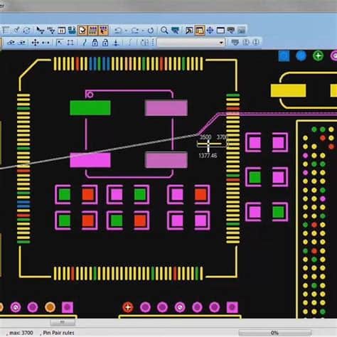
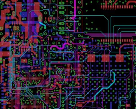
3. PCB layout
With the schematic and components in place, the designer can start working on the PCB layout. The layout process involves arranging the components on the board and routing the copper traces to connect them according to the schematic. The goal is to create a compact, efficient, and manufacturable layout while minimizing signal interference and ensuring proper power distribution.
4. Design rule check (DRC)
After completing the PCB layout, it’s crucial to perform a design rule check (DRC). A DRC is an automated process that verifies the layout against a set of predefined design rules, such as minimum trace width, clearance between components, and hole sizes. Running a DRC helps identify and correct any design issues before proceeding to fabrication.
5. Gerber file generation
Once the PCB layout passes the DRC, the designer generates Gerber files. Gerber files are industry-standard files that contain all the necessary information for PCB fabrication, including the copper layers, solder mask, silkscreen, and drill holes. These files are sent to the PCB manufacturer for production.
Important Considerations in PCB Design
When designing a PCB, there are several key factors to consider to ensure optimal performance and reliability:
1. Signal integrity
Signal integrity refers to the quality of the electrical signals transmitted through the PCB. To maintain signal integrity, designers must consider factors such as trace width, spacing, and impedance matching. Proper grounding and shielding techniques should also be employed to minimize electromagnetic interference (EMI) and crosstalk between signals.
2. Power distribution
Efficient power distribution is essential for the proper functioning of the electronic circuit. Designers must ensure that the PCB has adequate copper pour for power and ground planes, and that the power traces are sized appropriately to handle the required current. Decoupling capacitors should be placed close to the power pins of ICs to minimize power supply noise.
3. Thermal management
Electronic components generate heat during operation, which can affect the performance and reliability of the circuit. Designers must consider the thermal characteristics of the components and the PCB to ensure proper heat dissipation. This may involve using thermal vias, heatsinks, or other cooling methods to prevent overheating.
4. Manufacturing considerations
To ensure that the PCB can be manufactured reliably and cost-effectively, designers must follow certain design guidelines. These include maintaining minimum trace widths and clearances, avoiding sharp angles in traces, and providing adequate space for component placement and soldering. It’s also important to consider the capabilities and limitations of the PCB fabrication and assembly processes.

Best Practices for PCB Design
Here are some best practices to follow when designing PCBs:
- Use a consistent naming convention for components and nets to improve readability and maintainability of the design.
- Keep the PCB layout organized and symmetrical, with components arranged in a logical manner based on their functionality.
- Minimize the use of vias, especially in high-speed signals, to reduce signal reflections and impedance mismatches.
- Use ground planes and power planes to provide a low-impedance return path for signals and to distribute power efficiently.
- Follow the manufacturer’s recommended footprints and pad sizes for components to ensure proper soldering and reliability.
- Verify the design using simulations and prototypes before proceeding to mass production to catch any issues early in the development process.
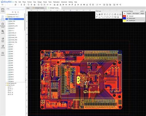
PCB Design Software
There are several PCB design software options available, ranging from free and open-source to commercial and enterprise-level solutions. Some popular PCB design software include:
| Software | Vendor | Pricing | Key Features |
|---|---|---|---|
| KiCad | KiCad | Free | Open-source, schematic and PCB layout, 3D viewer |
| EAGLE | Autodesk | Subscription-based | Schematic and PCB layout, extensive component libraries |
| Altium Designer | Altium | Subscription-based | Advanced features, multi-board design, simulation |
| OrCAD | Cadence | Subscription-based | Schematic and PCB layout, constraint-driven design |
When choosing a PCB design software, consider factors such as ease of use, feature set, pricing, and compatibility with your design requirements and workflow.
Frequently Asked Questions (FAQs)
1. What is the difference between a single-layer and multi-layer PCB?
A single-layer PCB has conductive traces on only one side of the board, while a multi-layer PCB has conductive traces on both sides and may also have internal layers. Multi-layer PCBs are used for more complex designs that require higher component density and better signal integrity.
2. What is the purpose of a solder mask on a PCB?
A solder mask is a protective layer applied to the copper traces on a PCB. It prevents accidental short circuits during soldering and protects the traces from oxidation and damage. The solder mask also provides insulation between adjacent traces and improves the aesthetics of the board.
3. What is the role of a silkscreen layer in PCB design?
The silkscreen layer is used to print text, logos, and component outlines on the PCB. It helps in identifying components, pin numbers, and other important information during assembly and troubleshooting. The silkscreen is typically applied on top of the solder mask and is usually white in color.
4. What are the common file formats used in PCB design?
The most common file formats used in PCB design are:
- Gerber files (.gbr): Contains information about the copper layers, solder mask, silkscreen, and drill holes.
- Drill files (.drl): Contains information about the size and location of the drill holes on the PCB.
- Bill of Materials (BOM): A list of all the components used in the design, including their quantities, part numbers, and values.
5. What is the importance of impedance matching in PCB design?
Impedance matching is crucial in high-speed PCB designs to ensure signal integrity and minimize reflections. When the impedance of a trace is not matched to the impedance of the source or load, signal reflections can occur, leading to signal distortion, noise, and other issues. Impedance matching involves controlling the width and spacing of the traces to achieve the desired impedance.
Conclusion
PCB design is a critical aspect of electronic product development, and understanding the basics is essential for new designers. By following the design process, considering important factors such as signal integrity and power distribution, and adhering to best practices, designers can create reliable and efficient PCBs. With the right tools and knowledge, anyone can start designing PCBs and bring their electronic ideas to life.
No responses yet