Introduction to PCB Design
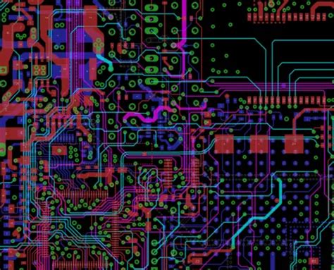
Printed Circuit Board (PCB) design is a crucial aspect of modern electronics manufacturing. It involves the creation of a layout for the electrical components and their interconnections on a board. The primary goal of PCB design is to ensure that the electronic device functions as intended while maintaining reliability, efficiency, and cost-effectiveness.
The Importance of PCB Design
PCB design plays a vital role in the overall performance and reliability of electronic devices. A well-designed PCB can:
- Minimize electromagnetic interference (EMI) and ensure signal integrity
- Improve heat dissipation and prevent overheating
- Reduce manufacturing costs and time-to-market
- Enhance the overall functionality and reliability of the device
The PCB Design Process
The PCB design process typically involves the following steps:
-
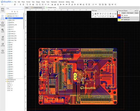
Schematic Design: The first step is to create a schematic diagram that represents the electrical connections between components. This is done using Electronic Design Automation (EDA) software.
-
Component Placement: Once the schematic is complete, the components are placed on the board layout. The placement is optimized for signal integrity, manufacturability, and ease of assembly.
-
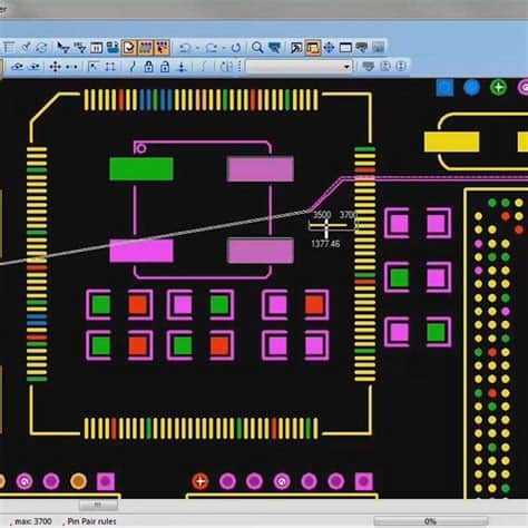
Routing: The next step is to route the connections between the components. This is done using copper traces on the board. The routing must follow design rules to ensure signal integrity and manufacturability.
-
Design Rule Check (DRC): After routing, a DRC is performed to ensure that the design meets all the required specifications and guidelines. This includes checking for proper spacing between traces, vias, and components.
-
Generate Manufacturing Files: Once the design is finalized, the manufacturing files are generated. These include Gerber files, drill files, and assembly drawings.
PCB Manufacturing Techniques
There are several techniques used in PCB manufacturing, each with its own advantages and limitations. The choice of manufacturing technique depends on factors such as the complexity of the design, the required precision, and the production volume.
Traditional PCB Manufacturing
Traditional PCB manufacturing involves the following steps:
-
Copper Clad Laminate: The process begins with a copper-clad laminate, which is a substrate material (usually FR-4) with a layer of copper on one or both sides.
-
Drilling: Holes are drilled into the laminate for through-hole components and vias.
-
Patterning: The copper layer is patterned using a photoresist and etching process. This creates the traces and pads on the board.
-
Plating: The holes are plated with copper to create electrical connections between layers.
-
Solder Mask and Silkscreen: A solder mask is applied to protect the copper traces, and a silkscreen is added for component labeling.
Advanced PCB Manufacturing Techniques
In addition to traditional manufacturing, there are several advanced techniques used for high-density and high-precision PCBs:
-
High Density Interconnect (HDI): HDI PCBs use microvias and fine-pitch traces to achieve higher component density and improved signal integrity.
-
Flexible PCBs: Flexible PCBs use a flexible substrate material, allowing the board to bend and conform to different shapes.
-
Rigid-Flex PCBs: Rigid-flex PCBs combine rigid and flexible sections, providing the benefits of both types of boards.
-
3D PCBs: 3D PCBs use multiple layers of flexible substrates to create three-dimensional structures, enabling more compact and complex designs.

PCB Materials and Properties
The choice of materials used in PCB manufacturing can have a significant impact on the performance and reliability of the final product. There are several key properties to consider when selecting PCB materials.
Substrate Materials
The most common substrate material used in PCB manufacturing is FR-4, a glass-reinforced epoxy laminate. Other substrate materials include:
- Polyimide: Used for high-temperature and flexible applications
- Teflon: Used for high-frequency and low-loss applications
- Ceramics: Used for high-power and high-frequency applications
Copper Thickness
The thickness of the copper layer on the PCB is an important consideration for current-carrying capacity and signal integrity. Common copper thicknesses include:
| Copper Weight (oz) | Thickness (μm) |
|---|---|
| 0.5 | 17.5 |
| 1 | 35 |
| 2 | 70 |
| 3 | 105 |
Solder Mask and Silkscreen
Solder mask and silkscreen are important for protecting the PCB and providing labeling for assembly. There are several types of solder mask and silkscreen materials, including:
- Liquid Photoimageable (LPI) solder mask: A photosensitive liquid that is applied and then exposed and developed to create the solder mask pattern
- Dry Film Solder Mask (DFSM): A dry film that is laminated onto the board and then exposed and developed
- Epoxy Ink: A screen-printable ink that is cured to create the silkscreen labeling

PCB Assembly Techniques
Once the PCB is manufactured, the components must be assembled onto the board. There are several techniques used for PCB assembly, each with its own advantages and limitations.
Through-Hole Assembly
Through-hole assembly involves inserting component leads through holes in the board and soldering them in place. This technique is used for larger components and provides a strong mechanical connection. However, it is slower and more labor-intensive than surface-mount assembly.
Surface-Mount Assembly
Surface-mount assembly involves placing components directly onto pads on the surface of the board and soldering them in place. This technique is faster and more automated than through-hole assembly, and allows for higher component density. However, it requires more precise placement and can be more difficult to rework.
Mixed Assembly
Mixed assembly combines through-hole and surface-mount components on the same board. This technique is used when some components are not available in surface-mount packages, or when a stronger mechanical connection is required for certain components.

PCB Testing and Inspection
After assembly, the PCB must be tested and inspected to ensure that it functions as intended and meets all required specifications. There are several techniques used for PCB testing and inspection.
Automated Optical Inspection (AOI)
AOI uses cameras and image processing software to inspect the PCB for defects such as missing components, incorrect placement, and solder bridging. AOI is fast and accurate, but cannot detect all types of defects.
X-Ray Inspection
X-ray inspection uses X-rays to image the internal structure of the PCB, allowing for the detection of defects such as voids in solder joints and broken traces. X-ray inspection is more expensive than AOI, but can detect defects that are not visible on the surface.
In-Circuit Testing (ICT)
ICT uses a bed-of-nails fixture to make electrical contact with the PCB and test the functionality of individual components and circuits. ICT is a comprehensive test that can detect a wide range of defects, but requires a custom fixture for each PCB design.
Functional Testing
Functional testing involves powering up the PCB and testing its overall functionality and performance. This can include tests such as boundary scan, JTAG, and built-in self-test (BIST). Functional testing is the final step in the testing process and ensures that the PCB meets all required specifications.
PCB Design and Manufacturing Challenges
Despite advances in PCB design and manufacturing technology, there are still several challenges that must be addressed to ensure the reliability and performance of electronic devices.
Signal Integrity
As PCBs become more complex and operate at higher frequencies, maintaining signal integrity becomes increasingly challenging. This requires careful design techniques such as impedance matching, differential signaling, and proper grounding and shielding.
Thermal Management
As electronic devices become more powerful and compact, managing heat dissipation becomes a critical challenge. This requires the use of thermal management techniques such as heatsinks, fans, and thermal vias.
Electromagnetic Compatibility (EMC)
EMC refers to the ability of electronic devices to operate without causing or being affected by electromagnetic interference. This requires careful design techniques such as proper grounding, shielding, and filtering.
Cost and Time-to-Market
In today’s competitive market, reducing costs and time-to-market are critical challenges for PCB designers and manufacturers. This requires the use of advanced design and manufacturing techniques such as design for manufacturability (DFM), panelization, and automation.
Future Trends in PCB Design and Manufacturing
As technology continues to advance, there are several emerging trends in PCB design and manufacturing that are likely to shape the future of the industry.
3D Printing
3D printing technology is increasingly being used for PCB Prototyping and low-volume production. This allows for faster turnaround times and greater design flexibility, but is currently limited by the available materials and resolution.
Embedded Components
Embedding components within the PCB substrate can provide several benefits, including reduced size, improved signal integrity, and enhanced thermal management. This technique is currently limited by the available materials and manufacturing processes, but is likely to become more widespread in the future.
High-Frequency Materials
As electronic devices operate at higher frequencies, the demand for high-frequency materials such as low-loss laminates and high-frequency ceramics is increasing. These materials provide improved signal integrity and reduced losses, but are more expensive than traditional materials.
Sustainability
There is growing concern about the environmental impact of electronic waste, and PCB designers and manufacturers are under increasing pressure to adopt sustainable practices. This includes the use of recycled materials, the elimination of hazardous substances, and the design of products for easy disassembly and recycling.
FAQs
- What is the difference between a single-sided and double-sided PCB?
-
A single-sided PCB has components and traces on only one side of the board, while a double-sided PCB has components and traces on both sides. Double-sided PCBs provide more space for components and routing, but are more complex and expensive to manufacture.
-
What is the purpose of vias in a PCB?
-
Vias are small holes drilled through the PCB that allow electrical connections to be made between layers. They are used to route signals between layers and to connect components on opposite sides of the board.
-
What is the difference between a standard and high-density PCB?
-
A standard PCB has a minimum trace width and spacing of about 8 mils (0.2 mm), while a high-density PCB has a minimum trace width and spacing of 4 mils (0.1 mm) or less. High-density PCBs allow for more complex designs and higher component density, but are more expensive and difficult to manufacture.
-
What is the purpose of a solder mask on a PCB?
-
A solder mask is a thin layer of polymer that covers the copper traces on a PCB, leaving only the pads and vias exposed. It serves to protect the traces from damage and prevent solder bridging during assembly.
-
What is the difference between through-hole and surface-mount assembly?
- Through-hole assembly involves inserting component leads through holes in the PCB and soldering them in place, while surface-mount assembly involves placing components directly onto pads on the surface of the board and soldering them in place. Surface-mount assembly allows for higher component density and faster assembly, but requires more precise placement and can be more difficult to rework.
Conclusion
PCB design and manufacturing are critical aspects of modern electronics that require a deep understanding of materials, processes, and techniques. As technology continues to advance, PCB designers and manufacturers must stay up-to-date with the latest trends and challenges to ensure the reliability, performance, and sustainability of electronic devices. By adopting best practices and embracing new technologies, the PCB industry can continue to drive innovation and meet the growing demands of the electronics market.

No responses yet