Introduction to Hyperspectral Imaging and PCB Design
Hyperspectral imaging (HSI) is a powerful technique that combines spectroscopy and imaging to capture detailed spectral information across a wide range of wavelengths for each pixel in an image. This technology has found applications in various fields, including remote sensing, agriculture, medical imaging, and material science. To effectively implement hyperspectral imaging systems, proper PCB design and layout are crucial. In this article, we will explore the key aspects of PCB design and layout for hyperspectral imaging systems, including the challenges, best practices, and considerations for optimizing system performance.
What is Hyperspectral Imaging?
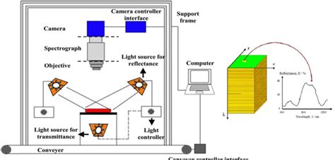
Hyperspectral imaging is an advanced imaging technique that captures spectral information beyond the visible light spectrum. Unlike traditional imaging methods that capture three color bands (red, green, and blue), hyperspectral imaging captures hundreds or even thousands of narrow spectral bands across a wide range of wavelengths, including visible, near-infrared, and short-wave infrared regions. This high-dimensional spectral data enables the identification and analysis of materials, objects, and phenomena based on their unique spectral signatures.
Importance of PCB Design in Hyperspectral Imaging Systems
The performance and reliability of hyperspectral imaging systems heavily rely on the proper design and layout of printed circuit boards (PCBs). PCBs serve as the backbone of these systems, connecting and integrating various components such as sensors, optical elements, data acquisition units, and processing units. A well-designed PCB ensures optimal signal integrity, power distribution, thermal management, and mechanical stability, which are essential for acquiring high-quality hyperspectral data.
Challenges in PCB Design for Hyperspectral Imaging Systems
Designing PCBs for hyperspectral imaging systems presents several challenges due to the complex nature of the technology and the stringent requirements for data acquisition and processing. Some of the key challenges include:
Signal Integrity
Hyperspectral imaging systems deal with high-speed and high-resolution data, which requires careful management of signal integrity. The PCB layout must minimize crosstalk, reflections, and electromagnetic interference (EMI) to ensure clean and accurate signal transmission. Proper impedance matching, trace routing, and shielding techniques are essential to maintain signal integrity.
Power Distribution
Hyperspectral imaging systems often consist of multiple components with varying power requirements. The PCB design must ensure stable and efficient power distribution to all components while minimizing noise and voltage fluctuations. Proper power plane design, decoupling capacitors, and voltage regulation techniques are crucial for reliable system operation.
Thermal Management
The high-performance components used in hyperspectral imaging systems, such as sensors, FPGAs, and processors, generate significant heat during operation. Effective thermal management is necessary to prevent overheating and ensure optimal performance. The PCB layout should incorporate proper heat dissipation techniques, such as thermal vias, heat sinks, and cooling mechanisms, to maintain acceptable operating temperatures.
Mechanical Stability
Hyperspectral imaging systems may be subjected to various environmental conditions, such as vibrations, shocks, and temperature variations. The PCB design must consider mechanical stability to withstand these conditions and maintain proper alignment of optical components. Robust mechanical mounting, strain relief, and appropriate material selection are essential for long-term reliability.
Best Practices for PCB Design and Layout in Hyperspectral Imaging Systems
To address the challenges and optimize the performance of hyperspectral imaging systems, several best practices should be followed in PCB design and layout. These practices ensure signal integrity, power integrity, thermal management, and mechanical stability.
Signal Integrity Techniques
-
Controlled Impedance: Match the impedance of the PCB traces to the characteristic impedance of the connected components and transmission lines to minimize reflections and signal distortions.
-
Differential Signaling: Use differential signaling techniques, such as LVDS (Low-Voltage Differential Signaling), for high-speed data transmission to reduce noise and improve signal integrity.
-
Shielding: Implement shielding techniques, such as ground planes, guard traces, and shielded connectors, to minimize electromagnetic interference (EMI) and crosstalk between signal traces.
-
Trace Routing: Follow proper trace routing guidelines, such as minimizing trace length, avoiding sharp bends, and maintaining consistent trace width and spacing, to reduce signal reflections and crosstalk.
Power Distribution Techniques
-
Power Plane Design: Use solid power planes instead of thin traces to provide low-impedance power distribution and minimize voltage drops.
-
Decoupling Capacitors: Place decoupling capacitors close to the power pins of components to suppress high-frequency noise and provide a stable power supply.
-
Voltage Regulation: Implement voltage regulation techniques, such as using low-dropout (LDO) regulators or switching regulators, to provide stable and clean power to sensitive components.
-
Power Sequencing: Ensure proper power sequencing for components with specific power-up requirements to avoid damage or erratic behavior.
Thermal Management Techniques
-
Thermal Vias: Use thermal vias to conduct heat from hot components to the ground plane or heat sink for efficient heat dissipation.
-
Component Placement: Strategically place components to minimize thermal coupling and ensure adequate airflow for cooling.
-
Heat Sinks: Incorporate heat sinks or thermal pads for components with high heat generation to enhance heat dissipation.
-
Thermal Simulation: Perform thermal simulations during the design phase to identify potential hot spots and optimize the PCB layout for effective thermal management.
Mechanical Stability Techniques
-
Robust Mounting: Use robust mechanical mounting techniques, such as screws, standoffs, or adhesives, to securely fasten components and prevent movement or vibration.
-
Strain Relief: Incorporate strain relief mechanisms for connectors and cables to prevent mechanical stress on the PCB and ensure reliable connections.
-
Material Selection: Choose appropriate PCB materials with suitable mechanical properties, such as high glass transition temperature (Tg) and low coefficient of thermal expansion (CTE), to withstand environmental stresses.
-
Vibration Damping: Implement vibration damping techniques, such as using rubber mounts or damping materials, to reduce the impact of vibrations on sensitive components.

Considerations for Specific Hyperspectral Imaging Applications
Different hyperspectral imaging applications may have specific requirements and considerations for PCB design and layout. Let’s explore a few common applications and their unique considerations.
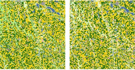
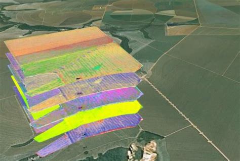
Remote Sensing
In remote sensing applications, hyperspectral imaging systems are often deployed on airborne or satellite platforms. Key considerations for PCB design in these applications include:
- Compact and lightweight design to minimize payload weight and size
- Rugged construction to withstand harsh environmental conditions, such as extreme temperatures and vibrations
- Efficient power management to optimize battery life and thermal performance
- High-speed data interfaces and storage solutions to handle large volumes of hyperspectral data
Medical Imaging
Hyperspectral imaging has shown promise in medical applications, such as cancer detection and tissue characterization. PCB design considerations for medical imaging include:
- Compliance with medical device regulations and standards, such as IEC 60601 for electrical safety and electromagnetic compatibility
- High signal-to-noise ratio (SNR) to capture subtle spectral variations in biological tissues
- Miniaturized and flexible PCB designs to integrate with endoscopic or handheld imaging probes
- Biocompatible materials and coatings to ensure patient safety and minimize contamination risks
Agricultural Monitoring
Hyperspectral imaging is used in precision agriculture to monitor crop health, soil conditions, and water stress. PCB design considerations for agricultural monitoring include:
- Rugged and waterproof enclosures to protect electronics from dust, moisture, and chemicals
- Wireless communication interfaces, such as Wi-Fi or LoRa, for remote data transmission and control
- Integration with sensor networks and IoT platforms for real-time monitoring and data analytics
- Low-power design to enable long-term deployment in field conditions
Industrial Inspection
Hyperspectral imaging is employed in industrial applications for quality control, material identification, and defect detection. PCB design considerations for industrial inspection include:
- High-speed data acquisition and processing to enable real-time inspection on production lines
- Robust connectors and interfaces to withstand industrial environments and frequent connections/disconnections
- Compatibility with industrial communication protocols, such as Ethernet, RS-485, or EtherCAT
- Modular design to facilitate system upgrades and customization for specific inspection tasks
FAQs
-
Q: What is the difference between hyperspectral imaging and multispectral imaging?
A: Hyperspectral imaging captures a much larger number of narrow spectral bands (typically hundreds or thousands) compared to multispectral imaging, which captures a smaller number of wider spectral bands (usually less than 20). This allows hyperspectral imaging to provide more detailed spectral information and enables finer discrimination of materials and objects. -
Q: What are the key components of a hyperspectral imaging system?
A: The key components of a hyperspectral imaging system typically include an imaging sensor (such as a CCD or CMOS), a spectrograph or spectral filter for wavelength separation, an optical system for image formation, a data acquisition unit, a processing unit, and storage devices. Additional components may include illumination sources, cooling systems, and mechanical mounts. -
Q: How does PCB material selection affect the performance of hyperspectral imaging systems?
A: The choice of PCB material can impact signal integrity, thermal management, and mechanical stability. Materials with low dielectric constant and loss, such as Rogers or PTFE-based laminates, are preferred for high-speed signals to minimize signal distortions. Materials with high thermal conductivity, such as metal-core PCBs or ceramic substrates, can enhance heat dissipation. Additionally, materials with low CTE and high Tg provide better mechanical stability under temperature variations. -
Q: What are the challenges in designing compact and lightweight PCBs for hyperspectral imaging systems?
A: Designing compact and lightweight PCBs for hyperspectral imaging systems requires careful consideration of component placement, routing density, and layer stackup. High-density interconnect (HDI) techniques, such as microvias and blind/buried vias, can be employed to minimize PCB size. Advanced packaging technologies, such as chip-on-board (COB) or ball grid array (BGA), can further reduce footprint. However, these techniques may increase design complexity and manufacturing costs. -
Q: How can simulation tools assist in PCB design for hyperspectral imaging systems?
A: Simulation tools play a crucial role in optimizing PCB design for hyperspectral imaging systems. Signal integrity simulations help analyze and mitigate issues like crosstalk, reflections, and EMI. Power integrity simulations ensure stable and clean power distribution. Thermal simulations identify hot spots and guide the placement of components and cooling solutions. Mechanical simulations assess the PCB’s structural integrity under various stress conditions. These simulations enable designers to make informed decisions and optimize the PCB layout before physical prototyping.
Conclusion
PCB design and layout are critical aspects of developing high-performance and reliable hyperspectral imaging systems. By understanding the challenges and applying best practices in signal integrity, power distribution, thermal management, and mechanical stability, designers can create PCBs that meet the stringent requirements of hyperspectral imaging applications. Consideration of application-specific factors, such as environmental conditions, data acquisition speed, and regulatory compliance, further enhances the PCB design process.
As hyperspectral imaging technology continues to advance and find new applications, PCB designers must stay updated with the latest techniques, materials, and tools to deliver cutting-edge solutions. Collaboration between imaging experts, system engineers, and PCB designers is essential to ensure optimal integration and performance of hyperspectral imaging systems.
By following the guidelines and best practices discussed in this article, designers can create robust and efficient PCBs that enable the full potential of hyperspectral imaging technology, driving innovation and unlocking new possibilities in various fields, from remote sensing and medical imaging to agriculture and industrial inspection.
No responses yet