What is 3D Viewing in PCB Design?
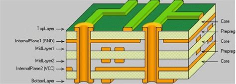
3D viewing in PCB design refers to the ability to visualize your PCB layout in a three-dimensional space. This feature allows you to see how your components, traces, and other elements will fit together in the final product. With 3D viewing, you can identify potential issues early in the design process, such as component clearance problems or signal integrity concerns.
Benefits of 3D Viewing in PCB Design
-
Improved Visualization: 3D viewing provides a more realistic representation of your PCB, making it easier to understand how everything fits together.
-
Early Error Detection: By visualizing your PCB in 3D, you can identify potential issues, such as component collisions or insufficient clearances, before moving to the manufacturing stage.
-
Enhanced Collaboration: 3D models can be shared with team members, stakeholders, and manufacturers, facilitating better communication and collaboration throughout the design process.
-
Increased Efficiency: With 3D viewing, you can make informed decisions faster, reducing the time and effort required to complete your PCB design.
Altium Designer’s 3D Viewing Capabilities
Altium Designer offers a robust set of 3D viewing features that can help you streamline your PCB design process and achieve better results.
Real-Time 3D Visualization
Altium Designer provides real-time 3D visualization of your PCB layout, allowing you to see the effects of your design changes instantly. This feature enables you to make informed decisions quickly and reduces the risk of errors.
Realistic Component Representation
With Altium Designer’s 3D viewing, you can see realistic representations of your components, including their dimensions, colors, and shapes. This feature helps you ensure that your components will fit together properly and that there are no clearance issues.
3D Measurements and Analysis
Altium Designer allows you to take measurements and perform analyses directly in the 3D view. You can measure distances, angles, and clearances, as well as check for potential signal integrity issues.
3D STEP Model Export
Altium Designer enables you to export your PCB design as a 3D STEP model, which can be shared with manufacturers or used for further analysis in other software tools.

How 3D Viewing in Altium Designer Improves Your PCB Design Process
Implementing 3D viewing in your PCB design process with Altium Designer can lead to significant improvements in efficiency, accuracy, and overall quality.
Faster Iteration and Refinement
With real-time 3D visualization, you can quickly iterate and refine your PCB layout, making adjustments as needed to optimize performance and minimize potential issues.
Reduced Risk of Errors
By identifying potential problems early in the design process, 3D viewing helps reduce the risk of costly errors that may not be discovered until the manufacturing stage.
Improved Collaboration and Communication
3D models can be easily shared with team members, stakeholders, and manufacturers, facilitating better communication and collaboration throughout the design process.
Streamlined Manufacturing Preparation
Exporting your PCB design as a 3D STEP model allows you to provide manufacturers with a clear and accurate representation of your design, reducing the likelihood of misinterpretation or errors during production.

Real-World Examples of 3D Viewing in Altium Designer
To illustrate the benefits of 3D viewing in Altium Designer, let’s look at some real-world examples.
Example 1: Identifying Component Clearance Issues
An electronics engineer is designing a compact PCB for a wearable device. By using Altium Designer’s 3D viewing capabilities, they discover that two components are too close together, which could lead to signal integrity issues and potential device failure. By identifying this issue early in the design process, the engineer can make the necessary adjustments to ensure proper clearances and optimal performance.
Example 2: Collaborating with Manufacturers
A PCB design team is working on a complex, multi-layer board for an industrial control system. By exporting their design as a 3D STEP model, they can provide their manufacturing partners with a clear and accurate representation of the PCB. This improved communication helps ensure that the final product meets the design specifications and reduces the risk of manufacturing errors.
Example 3: Optimizing Component Placement
A designer is working on a high-speed PCB for a telecommunications application. Using Altium Designer’s 3D viewing and measurement tools, they can optimize the placement of critical components to minimize signal path lengths and reduce the risk of signal integrity issues. This optimization helps improve the overall performance and reliability of the final product.

Frequently Asked Questions (FAQ)
-
Is 3D viewing available in all versions of Altium Designer?
Yes, 3D viewing is a standard feature in all versions of Altium Designer. -
Can I export my PCB design as a 3D model in formats other than STEP?
Yes, Altium Designer supports exporting 3D models in various formats, including STEP, IGES, and OBJ. -
Does 3D viewing in Altium Designer require any additional hardware or software?
No, 3D viewing is fully integrated into Altium Designer and does not require any additional hardware or software. -
Can I use 3D viewing to check for signal integrity issues?
Yes, Altium Designer’s 3D viewing tools allow you to perform various analyses, including signal integrity checks. -
How can I learn more about using 3D viewing in Altium Designer?
Altium provides extensive documentation, tutorials, and webinars to help users learn and master the 3D viewing features in Altium Designer. You can also reach out to the Altium support team or community forums for guidance and assistance.
Conclusion
3D viewing is a powerful feature in PCB design that can help you streamline your design process, reduce the risk of errors, and improve the overall quality of your PCBs. Altium Designer offers a comprehensive set of 3D viewing capabilities, including real-time visualization, realistic component representation, and 3D measurement and analysis tools. By leveraging these features, you can make informed decisions faster, collaborate more effectively with team members and manufacturers, and ultimately create better PCB designs.
| Advantage | Description |
|---|---|
| Improved Visualization | 3D viewing provides a more realistic representation of your PCB, making it easier to understand how everything fits together. |
| Early Error Detection | By visualizing your PCB in 3D, you can identify potential issues, such as component collisions or insufficient clearances, before moving to the manufacturing stage. |
| Enhanced Collaboration | 3D models can be shared with team members, stakeholders, and manufacturers, facilitating better communication and collaboration throughout the design process. |
| Increased Efficiency | With 3D viewing, you can make informed decisions faster, reducing the time and effort required to complete your PCB design. |
As PCB designs continue to become more complex and compact, the importance of 3D viewing in the design process will only continue to grow. By embracing the powerful 3D viewing capabilities offered by Altium Designer, you can position yourself and your team for success in the ever-evolving world of PCB design.

No responses yet