Introduction to Printed Circuit Boards (PCBs)
A Printed Circuit Board, commonly referred to as a PCB, is the backbone of modern electronic devices. It is a flat board made of insulating material, such as fiberglass or composite epoxy, with conductive copper traces etched onto its surface. These traces connect various electronic components, such as resistors, capacitors, and integrated circuits (ICs), to form a complete electronic circuit.
PCBs have revolutionized the electronics industry by providing a reliable, compact, and cost-effective means of assembling electronic circuits. They are found in virtually all electronic devices, from simple toys and household appliances to complex medical equipment, computers, and aerospace systems.
History of PCBs
The concept of printed circuits dates back to the early 20th century. In 1903, German inventor Albert Hanson filed a patent for a “printed wire” that described a method of stamping conductive traces onto an insulating board. However, it wasn’t until the 1920s that the first practical printed circuits were developed.
In 1936, Austrian engineer Paul Eisler invented the first printed circuit board while working on a radio set. He used a copper foil-clad base board and printed the wiring pattern using a stencil. This method laid the foundation for modern PCB manufacturing.
During World War II, PCBs were extensively used in military equipment, such as proximity fuses for artillery shells, due to their compact size and reliability. After the war, PCBs found applications in consumer electronics, and their use continued to grow with the advent of transistors and integrated circuits in the 1950s and 1960s.

PCB Manufacturing Process
The PCB manufacturing process involves several steps, each of which is critical to ensuring the quality and reliability of the final product. The main stages of PCB manufacturing are:
-
Design: The PCB design is created using specialized software, such as Altium Designer or Eagle. The design includes the schematic diagram, component placement, and routing of the copper traces.
-
Printing: The PCB design is printed onto a transparent film or photomask, which is used to transfer the pattern onto the copper-clad board.
-
Etching: The copper-clad board is coated with a light-sensitive photoresist and exposed to UV light through the photomask. The exposed areas of the photoresist are then removed, revealing the copper traces underneath. The board is then submerged in an etchant solution, which removes the unwanted copper, leaving only the desired traces.
-
Drilling: Holes are drilled into the board to accommodate through-hole components and provide electrical connections between layers in multi-layer PCBs.
-
Plating: The holes are plated with copper to ensure electrical continuity between layers. Additional protective coatings, such as solder mask and silkscreen, may also be applied.
-
Assembly: Electronic components are soldered onto the PCB, either manually or using automated pick-and-place machines.
-
Testing: The assembled PCB undergoes various tests, such as visual inspection, automated optical inspection (AOI), and electrical testing, to ensure proper functionality and quality.

Types of PCBs
PCBs can be classified based on various factors, such as the number of layers, the type of material used, and the assembly method. Some common types of PCBs include:
Single-Sided PCBs
Single-sided PCBs have conductive traces on only one side of the insulating substrate. They are the simplest and most cost-effective type of PCB, suitable for low-complexity circuits and low-volume production.
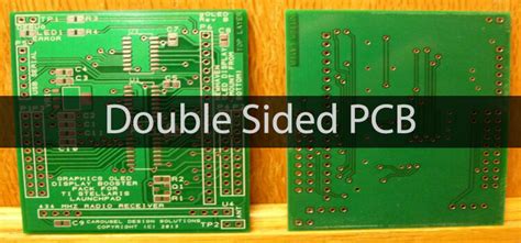
Double-sided PCBs
Double-sided PCBs have conductive traces on both sides of the insulating substrate, allowing for higher component density and more complex circuits compared to single-sided PCBs. The two layers are connected using through-hole vias.
Multi-layer PCBs
Multi-layer PCBs consist of three or more conductive layers separated by insulating layers. They offer the highest component density and are used in complex, high-performance applications, such as computer motherboards and telecommunications equipment.
| PCB Type | Layers | Complexity | Cost | Applications |
|---|---|---|---|---|
| Single-sided | 1 | Low | Low | Simple circuits, low-volume production |
| Double-sided | 2 | Medium | Medium | More complex circuits, moderate-volume production |
| Multi-layer | 3+ | High | High | High-performance, complex circuits, high-volume production |
Rigid PCBs
Rigid PCBs are made using a solid, inflexible substrate material, such as FR-4 fiberglass. They are the most common type of PCB and are used in a wide range of applications, from consumer electronics to industrial equipment.
Flexible PCBs
Flexible PCBs, also known as flex circuits, are made using a flexible substrate material, such as polyimide or polyester. They can bend and twist without damaging the conductive traces, making them ideal for applications with limited space or moving parts, such as cameras, wearable devices, and automotive electronics.
Rigid-Flex PCBs
Rigid-flex PCBs combine the benefits of both rigid and flexible PCBs. They consist of rigid sections connected by flexible sections, allowing for three-dimensional packaging and improved reliability in applications with high vibration or mechanical stress.
| PCB Type | Substrate Material | Flexibility | Applications |
|---|---|---|---|
| Rigid | FR-4, Fiberglass | Inflexible | Most common, wide range of applications |
| Flexible | Polyimide, Polyester | Highly flexible | Limited space, moving parts, wearables |
| Rigid-Flex | Combination of rigid and flexible materials | Partially flexible | 3D packaging, high vibration environments |

PCB Design Considerations
Designing a PCB involves several key considerations to ensure optimal performance, reliability, and manufacturability. Some of the main factors to consider when designing a PCB include:
Component Placement
Components should be placed in a logical and efficient manner, taking into account factors such as signal integrity, heat dissipation, and ease of assembly. Critical components, such as clocks and power regulators, should be placed close to their associated circuits to minimize noise and signal degradation.
Signal Integrity
Proper signal integrity is essential for ensuring reliable operation of the electronic circuit. This involves minimizing crosstalk, reflections, and electromagnetic interference (EMI) through techniques such as proper trace routing, impedance matching, and the use of ground planes and shielding.
Power Management
Efficient power distribution is crucial for maintaining stable operation and minimizing heat generation. This involves proper sizing of power traces, the use of decoupling capacitors to reduce noise, and the implementation of power planes for low-impedance power distribution.
Thermal Management
Heat generated by electronic components must be effectively dissipated to prevent overheating and ensure long-term reliability. This can be achieved through the use of heat sinks, thermal vias, and proper component placement to promote airflow.
Manufacturability
The PCB design must be compatible with the manufacturing process to ensure high yields and minimize production costs. This involves adhering to design rules, such as minimum trace widths and spacings, hole sizes, and soldermask clearances, as well as considering the capabilities of the chosen PCB manufacturer.
PCB Testing and Inspection
Thorough testing and inspection are essential for ensuring the quality and reliability of PCBs. Some common testing and inspection methods include:
Visual Inspection
Visual inspection is the first step in PCB testing and involves examining the board for obvious defects, such as missing components, solder bridges, or damaged traces. This can be done manually or using automated optical inspection (AOI) systems.
In-Circuit Testing (ICT)
In-circuit testing involves using a bed-of-nails fixture to make electrical contact with specific points on the PCB and verify the presence, orientation, and value of individual components. This method is useful for detecting component-level faults and ensuring proper assembly.
Flying Probe Testing
Flying probe testing uses movable test probes to make electrical contact with various points on the PCB. This method is more flexible than ICT and can be used for low-volume production or prototypes where the cost of a dedicated ICT fixture is not justified.
Functional Testing
Functional testing involves powering up the PCB and verifying that it performs its intended function. This can be done using automated test equipment (ATE) or by connecting the PCB to a test jig that simulates its operating environment.
Boundary Scan Testing
Boundary scan testing, also known as JTAG testing, is a method of testing complex digital circuits by accessing and controlling the boundary pins of integrated circuits. This allows for testing of individual components and interconnects without the need for physical access to the circuit board.
PCB Assembly Techniques
There are two main methods for assembling components onto a PCB:
Through-Hole Assembly
Through-hole assembly involves inserting component leads through holes drilled in the PCB and soldering them to pads on the opposite side. This method is suitable for larger components and provides a strong mechanical connection, but it is slower and more labor-intensive compared to surface-mount assembly.
Surface-Mount Assembly
Surface-mount assembly involves soldering components directly onto pads on the surface of the PCB. This method allows for smaller components and higher component density compared to through-hole assembly. Surface-mount assembly is faster and more automated, making it the preferred choice for high-volume production.
| Assembly Method | Component Size | Connection Strength | Speed | Automation |
|---|---|---|---|---|
| Through-Hole | Larger | Strong | Slower | Less automated |
| Surface-Mount | Smaller | Weaker | Faster | Highly automated |
Advantages of PCBs
PCBs offer several advantages over other methods of assembling electronic circuits, such as point-to-point wiring or wire-wrap. Some of the main benefits of using PCBs include:
-
Compact size: PCBs allow for high component density and efficient use of space, enabling the design of smaller and more portable electronic devices.
-
Reliability: PCBs provide a stable and reliable platform for electronic circuits, with fewer potential points of failure compared to other assembly methods.
-
Consistency: The automated manufacturing process ensures consistent quality and reproducibility, reducing the risk of human error and making PCBs suitable for high-volume production.
-
Cost-effective: PCBs are cost-effective for medium to high-volume production, as the initial setup costs are offset by the efficiency and speed of the manufacturing process.
-
Improved signal integrity: Proper PCB design techniques, such as controlled impedance and ground planes, help maintain signal integrity and reduce noise and interference.
Applications of PCBs
PCBs are used in a wide range of electronic applications, from consumer electronics to industrial equipment and aerospace systems. Some common applications include:
-
Consumer electronics: Smartphones, tablets, laptops, televisions, and home appliances.
-
Automotive electronics: Engine control units, infotainment systems, and advanced driver assistance systems (ADAS).
-
Medical devices: Diagnostic equipment, patient monitoring systems, and implantable devices.
-
Industrial automation: Programmable logic controllers (PLCs), robotics, and process control systems.
-
Aerospace and defense: Avionics, satellites, and military communication systems.
FAQ
What is the difference between a PCB and a PCBA?
A PCB (Printed Circuit Board) is the bare board with copper traces and pads, while a PCBA (Printed Circuit Board Assembly) is a PCB with electronic components soldered onto it, forming a complete Electronic Assembly.
What materials are PCBs made of?
PCBs are typically made of an insulating substrate material, such as FR-4 fiberglass or composite epoxy, with a layer of copper foil bonded to one or both sides. The copper layer is etched to form the conductive traces and pads.
How are PCBs designed?
PCBs are designed using specialized software, such as Altium Designer or Eagle. The design process involves creating a schematic diagram, laying out the components, and routing the copper traces. The design must adhere to various design rules and constraints to ensure manufacturability and reliability.
What is the difference between through-hole and surface-mount components?
Through-hole components have leads that are inserted into holes drilled in the PCB and soldered to pads on the opposite side. Surface-mount components are soldered directly onto pads on the surface of the PCB. Surface-mount components are smaller and allow for higher component density compared to through-hole components.
How are PCBs tested for quality and reliability?
PCBs undergo various tests to ensure quality and reliability, including visual inspection, automated optical inspection (AOI), in-circuit testing (ICT), flying probe testing, functional testing, and boundary scan testing. These tests help identify defects, verify proper assembly, and ensure that the PCB performs its intended function.
Conclusion
Printed Circuit Boards (PCBs) are the foundation of modern electronic devices, providing a reliable, compact, and cost-effective means of assembling electronic circuits. The development of PCBs has revolutionized the electronics industry, enabling the creation of increasingly complex and sophisticated devices.
Understanding the basics of PCBs, including their manufacturing process, design considerations, assembly techniques, and testing methods, is essential for anyone involved in the development or production of electronic products. As technology continues to advance, the role of PCBs in shaping the future of electronics will only become more significant.
No responses yet